





New nRF54L Series SoC with NPU and Nordic Edge AI Lab make ondevice intelligence easily accessible and radically power-efficient
Nordic Semiconductor is bringing AI intelligence and functionality to the smallest battery-powered IoT devices. With an industry-leading, ultra-lowpower Edge AI solution, Nordic accelerates the arrival of a new generation of devices with integrated edge AI intelligence – combining energy efficiency with unmatched ease of use for developers.
“AI factories train intelligence, but Nordic deploys it – on device, at the edge, where the world happens – said Vegard Wollan, CEO at Nordic Semiconductor. “Edge AI is no longer optional – it’s the only way to deliver safety, privacy, and sustainability at scale. Nordic’s edge AI solution enables millisecond decisions without round-trip latency to the cloud, ensures compliance through local processing, and delivers radically improved battery life for billions of connected devices. This is the new standard for ultra-low-power edge AI and Nordic is defining it.”
In 2023, Nordic acquired Atlazo and its Axon technology. The nRF54LM20B SoC is the first large-memory member of the nRF54L Series, integrating the Axon Neural Processing Unit (NPU), an ultra-efficient AI hardware accelerator, to supercharge demanding edge AI workloads. Axon delivers up to 7 times faster performance and up to 8 times higher energy efficiency versus competing solutions for tasks such as sound classification, keyword spotting, and image-based detection.



The nRF54LM20B SoC pairs the Axon NPU with 2 MB NVM, 512 KB RAM, a 128 MHz Arm® Cortex-M33 plus RISC-V coprocessor, high-speed USB, up to 66 GPIOs, and Nordic’s fourth-generation ultra-low-power 2.4 GHz radio supporting Bluetooth® LE, Bluetooth Channel Sounding, Matter over Thread, and more.
The Neuton models are ultra-tiny, CPUrun edge AI models that are typically under 5 KB and up to 10 times smaller, faster, and more efficient than other CPUrun models. Nordic Edge AI Lab helps developers generate custom Neuton models for anomaly detection, activity and gesture recognition, biometric monitoring, and more – delivering privacypreserving, real-time intelligence on tiny batteries and constrained memory, without cloud dependency.
With Nordic Edge AI Lab and Neuton models, intelligence moves from concept to reality without complexity. One recent deployment illustrates this: A global supply chain solution upgraded its smart tracking devices with AI models created in Nordic Edge AI Lab effortlessly, enabling detection of real handling events such as shock, shaking, and transportation directly on an nRF54L Series SoC. These AI-driven insights were rolled out across an entire fleet without operational disruption, thanks to Nordic’s nRF Cloud lifecycle services.


“With Nordic Edge AI Lab, Neuton models, and the Axon NPU, Nordic makes advanced on-device AI practical for every embedded developer,” said Oyvind Strom, EVP ShortRange BU at Nordic Semiconductor. “Developers get the simplicity to move fast, and the disruptive performance to scale from wearables to industrial sensing – all enabled within Nordic’s trusted ultra-lowpower hardware solutions.”
As intelligence moves to the edge, the need for OTA management and deep observability is growing. At the same time, cloudbased lifecycle services remain critical for device management, embedded observability, and location services. Manufacturers increasingly need continuous insight into device performance – not just to improve products in real time, but to meet growing regulatory and customer requirements. Using data from deployed devices enhances features and optimizes performance without disrupting the user experience. This ensures connected products can evolve securely and efficiently throughout their lifecycle.
Nordic Edge AI Lab and custom Neuton models are available today for Nordic wireless nRF54 Series SoCs and cellular IoT SiP modules. The nRF54LM20B SoC with Axon NPU is now sampling to selected customers, with broad availability for development expected early Q2 2026.
■ Nordic Semiconductor www.nordicsemi.com
3 | Nordic Semiconductor simplifies edge AI for billions of IoT devices
5 | Microchip Releases Custom Firmware For NVIDIA DGX Spark For Its MEC1723 Embedded Controllers
6 | Breakthrough in D-band Wireless: Anritsu and VTT Demonstrate World-Leading Transmitarray-Based High-Speed Connectivity
6 | New eBook from Mouser Provides an Engineering Guide to RF Design and Applications
7 | Portwell Acquires Major Stake in Wincomm to Enrich Scenario-Defined Appliance Solutions in Medical/ Healthcare and Industrial Markets
8 | Morse Micro MM8108 SoC, Now at Mouser, Delivers Next Generation Wi-Fi HaLow Performance for IoT Applications
8 | From immersive XR to advanced robotics and wearables: Bosch Sensortec launches BMI5 motion sensor platform
9 | Early Testing of Motor Control Units: Vector Introduces CANoe Model Option Electric Motor
10 | Allegro MicroSystems Sets New Standard for Efficiency in High-Power Systems with Ultra-Low-Loss Isolated Current Sensor
10 | Renesas Fast-Tracks SDV Innovation with R-Car Gen 5 SoC-Based End-to-End Multi-Domain Solution Platform
11 | Allegro MicroSystems Simplifies SiC Power Design for AI Data Centers and EVs with Expanded Power-Thru™ Gate Driver Portfolio


Enable low power inference capability in Edge AI applications
Mouser Electronics Signs Global Distribution Agreement with Telit Cinterion for Enterprise-Grade IoT Solutions
| Strengthening resilience amid Global Supply Chain Shocks
| Mouser


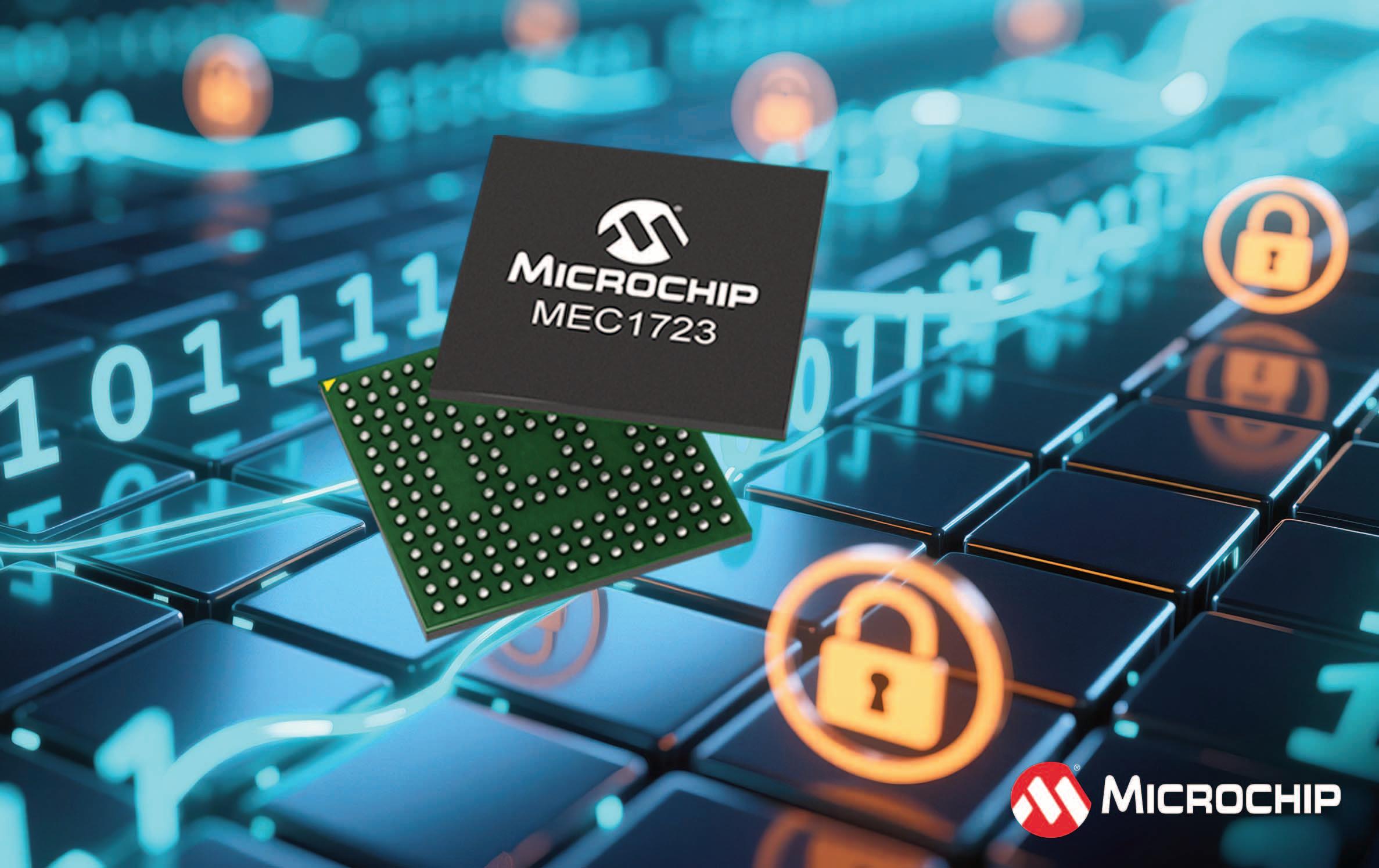
Microchip Technology has announced the release of custom-designed firmware for its MEC1723 Embedded Controller (EC), specifically tailored to support NVIDIA DGX Spark personal AI supercomputers. The software is designed to optimize the MEC1723 EC’s capabilities for system management of AI workloads on the NVIDIA DGX platform. By focusing on firmware innovation within its controllers, Microchip is helping to improve performance and security in demanding AI computing architectures.
Embedded controllers play an important role in managing power sequencing, alerts and system-level energy regulation. In this application, the MEC1723 EC goes a step further to also manage critical firmware operations.
• Secure firmware authentication: firmware code is digitally signed and authenticated by NVIDIA, helping to maintain platform integrity.


• Root of Trust for system boot: cryptographic verification of the firmware using Elliptic Curve Cryptography (ECC-P384) public key technology. This establishes the root of trust for the entire laptop, which is critical because the EC is the first device to power on and authorize secure system boot.
• Advanced power management: handles battery charging, alerts and system power state transitions to optimize energy efficiency.
• System control: oversees key scan and keypad operations for reliable user input.
• New host interface support: implements packet command format processing unique to the NVIDIA DGX interface, advancing beyond traditional byte-level data transfers.
• Value-added integration: incorporates Electromagnetic Interference (EMI) and Static Random-Access Memory (SRAM) interfaces to improve overall system performance.


“The collaboration between Microchip and NVIDIA helps deliver secure, tailored firmware solutions that address the complex needs of modern computing platforms,” said Nuri Dagdeviren, corporate vice president of Microchip Technology’s secure computing group. “Our MEC1723 firmware is customized to provide reliable operation and advanced functionality for NVIDIA DGX architecture, supporting the evolving requirements of client computing.”
Microchip’s MEC embedded controllers are designed to support the next generation of notebook and desktop applications across industrial, data center and consumer markets. These controllers provide advanced system management, security features and efficient power management, making them suitable for today’s high-performance computing needs. To learn more, download the MEC1723 EC datasheet.
■ Microchip Technology www.microchip.com
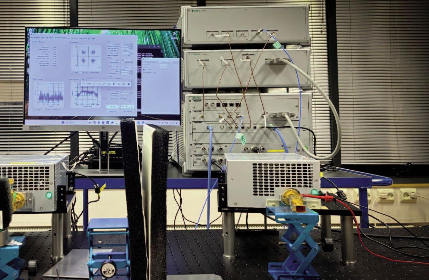
Anritsu and VTT Technical Research Centre of Finland have demonstrated a major advance in D-band wireless communications by validating a beam-steering transmitarray antenna system using advanced test equipment. The achievement confirms the feasibility of stable, high-capacity wireless links for next-generation backhaul, industrial, defense and future 6G networks.
Using Anritsu’s precision test equipment and VTT’s steerable transmitarray antenna, the teams achieved high-speed wireless links across the 110–170 GHz D-band. Link performance and beam-steering behavior were assessed under realistic over-the-air (OTA) conditions using wideband modulated signals up to 8 GHz bandwidth. This system-level characterization, from signal generation to OTA performance, confirmed multi-gigabit data rates in the tens-of-Gbps range, including 20 Gbps over 1 m and reliable operation up to 7 m, setting a new benchmark for D-band connectivity.
The demonstration features a lightweight, scalable transmitarray antenna developed by VTT, incorporating advanced phase-shifting elements and vector-modulator MMICs. Its electronically steerable design provides rapid, precise beam control without mechanical movement, maintaining signal strength under changing conditions. Supported by Anritsu’s state-of-the-art test equipment, the results reflect a proven, instrumentation grade measurement approach that ensures reliability and scalability for future deployments.
“Anritsu is proud to collaborate with VTT to advance the practical use of D-band wireless technology. Together, we have validated performance levels that bring high-frequency wireless links closer to real-world deployment,” said Jonathan Borrill, CTO, Test & Measurement, Anritsu.
“This milestone shows how strategic partnerships turn deep tech into competitive advantage. By combining VTT’s steerable transmitarray expertise with Anritsu’s precise instrumentation-grade validation, we shorten adoption cycles and scale D-band from the lab to live networks - creating growth opportunities across critical infrastructure, manufacturing, defense, 6G and beyond,” said Tauno Vähä-Heikkilä, Director, Strategic Partnerships, VTT.
■ Anritsu | www.anritsu.com

Mouser Electronics, Inc announces a new eBook, The RF Design Handbook: Theory, Components, and Applications. The eBook delves into key radio frequency (RF) design topics ranging from signal chain fundamentals and antenna selection to testing, certification, and digital integration.
Many of the devices and systems that people rely on for wireless communication, power transfer, navigation, and sensing operate within the RF spectrum. With such a diverse range of applications and markets, designing RF circuits can be a complex and nuanced process. The RF Design Handbook explains key concepts and provides engineers with the knowledge they need to get started. The eBook also explores the tools and components that will help engineers bring their ideas to life.
Among the new products featured in the eBook are the following:
• The WFI32E04UE Wi-Fi® microcontroller (MCU) module from Microchip Technology is a high-performance solution for industrial applications. The fully certified module supports 2.4 GHz 802.11 b/g/n radio modes and offers comprehensive WLAN functions for industry-leading connectivity. To ensure reliable and versatile wireless communication, the WFI32E04UE module supports AP, STA, SoftAP, TLS, and WPA/WPA2 modes. A U.FL antenna connector allows for connection to an external antenna.

• The GNSS L1 passive ceramic patch and chip antennas from TE Connectivity/Linx Technologies deliver high performance, reliability, and efficiency. The antennas operate within a frequency range of 1561 MHz to 1602 MHz and feature a 50-ohm impedance. Surface-mount and through-hole mount options are available. The GNSS L1 antennas are suitable for applications including asset tracking, precision surveying, and Global Navigation Satellite Systems (GNSS).
• The High-Speed FAKRA-Mini (HFM) interconnect system by Molex provides a compact, high-performance solution for modern vehicle architectures. The HFM connectors support data rates of up to 28 Gbps at frequencies of up to 20 GHz. Featuring a compact form factor, the HFM connectors reduce weight, save installation space, and maximize limited PCB real estate. The High-Speed FAKRA-Mini HFM interconnect system is ideal for applications including internet connections, infotainment systems, 5G, Bluetooth®, and Wi-Fi.
• The EFR32BG29 series 2 Bluetooth wireless SoCs from Silicon Labs are an advanced, ultra-low-power solution designed for high-performance wireless applications. The EFR32BG29 SoCs feature a powerful 76.8 MHz Arm® Cortex®-M33 core, providing sufficient processing power for complex applications while maintaining energy efficiency. Featuring a 2.4 GHz radio with excellent sensitivity, the EFR32BG29 Series 2 SoCs are an ideal choice for reliable, long-range connectivity.
– To read the new eBook, visit https://resources.mouser.com/rf-wireless/rf-design-hand book-theory-components-applications
– To browse Mouser’s extensive eBook library, visit https://resources.mouser.com/manufacturer-ebooks
– For more Mouser news and our latest new product introductions, visit www.mouser.com/newsroom
■ Mouser Electronics | www.mouser.com


Portwell Acquires Major Stake in Wincomm to Enrich Scenario-Defined Appliance Solutions in Medical/ Healthcare and Industrial Markets
Portwell, Inc. announced its strategic investment in Wincomm Corporation, acquiring a 41% ownership stake and becoming its major shareholder. Wincomm Corporation, headquartered in Hsinchu, Taiwan, is a wellestablished innovator in the touchscreen computer market, with a strong foothold in medical equipment, smart healthcare and industrial automation sectors. Its diverse HumanMachine Interface (HMI) computer and display portfolio includes medical-grade panel PCs, embedded touch displays, and peripherals, as well as rugged industrial-grade solutions such as wide-temperature and high-brightness panel PCs, waterproof stainless-steel displays, and IECEx, ATEX, C1D2/C2D2-certified explosion-proof panel PCs.
“This investment marks a significant milestone in Portwell’s growth direction,” said Ken Guan, President of Portwell, Inc
“By joining forces with Wincomm, we are not only reinforcing our presence in the medical computing space but also expanding our capabilities across factory automation, petrochemical, and military applications. The synergy between our product lines and business models will enhance our overall competitiveness and customer satisfaction, while driving innovation in Edge AI and embedded computing.”
“Portwell’s strategic investment strengthens Wincomm’s foundation to achieve its vision of becoming a global leader in medical and industrial Edge AI solutions within the next 3–5 years,” said HY Chiou, CEO of Wincomm. “With Portwell’s support, we can optimize cost structures, enhance system production quality, and leverage its global network to expand international business,” he added. Chiou emphasized that the collaboration will accelerate embedded technology development - including high performance GPU/AI chip, ARM, Linux, and Androidexpanding Wincomm’s Edge AI product capabilities.”
Scenario-defined Embedded Appliance Solutions and AIoT Edge Compute form the core of Portwell’s technology and business strategy. The acquisition aligns with Portwell’s long-term vision to deliver comprehensive, application-ready solutions across diverse verticals. With Wincomm’s proven expertise and product innovation, Portwell is poised to accelerate its impact in smart healthcare and industrial automation markets worldwide.
■ Portwell | www.portwell.eu
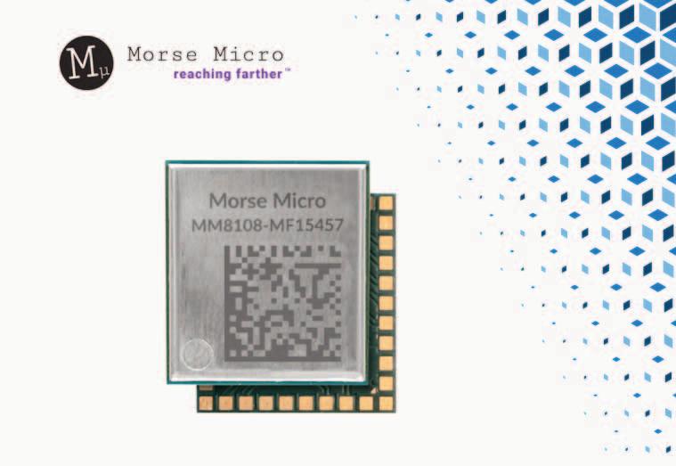
Mouser Electronics is now shipping the new MM8108 Wi-Fi® HaLow® System-on-chip (SoC) from Morse Micro. The MM8108 SoC is a HaLow-compliant connectivity solution tailored to meet the needs of Internet of Things (IoT) and machine-to-machine (M2M) applications.
The Morse Micro MM8108 SoC, available from Mouser, is a highly integrated, ultra-low-power, single-chip Wi-Fi solution offering improved performance in all key areas, including range, throughput, and power efficiency, while also reducing the cost, effort, and time required to bring the next generation of Wi-Fi HaLow-enabled products to market. Wi-Fi HaLow is the first Wi-Fi standard tailored to meet the needs of IoT applications, and the MM8108 delivers over-the-air data rates up to 43.33Mbps at 8MHz bandwidth in worldwide sub-GHz license-exempt bands, with next-generation upgrades boasting 16x better efficiency than standard Wi-Fi.
The MM8108 adds an integrated high-efficiency power amplifier (PA) and high-linearity low-noise amplifier (LNA) that meet the IEEE 802.11ah standard, while integrating full MAC and PHY implementations. The MM8108’s RF interface can also be configured with an external PCB-mount PA or front-end module (FEM) for ultra-long-reach applications with leading Wi-Fi HaLow security features (WPA3, SAE, GCMP) to ensure link-layer communications start and remain protected.
Mouser also stocks several evaluation kits for the MM8108 SoC. The Morse Micro MM8108-EKH01-01 kits offer a prototyping platform based on the Raspberry Pi 4B. The MM8108EKH05-01 evaluation kit is a fully integrated development platform for a wide range of IoT applications featuring an MM8108 SoC, an STM32U585 low-power microcontroller (MCU), and a BlueNRG-M2 Bluetooth® SoC. The MM8108EKH19 kit features a USB 2.0 network adapter reference design based on the MM8108 SoC, an SMA Wi-Fi HaLow antenna, and a GL-MT3000 router.
■ Mouser Electronics | www.mouser.com

Immersive XR systems, agile robots and feature-rich wearables rely on motion data that remains stable even when environments become dynamic. As device capabilities grow, so do the demands placed on their sensing technology. At CES 2026, Bosch Sensortec introduces the BMI5 platform, a new generation of inertial sensors designed to provide consistent, high-precision performance across multiple device classes. Built on a shared hardware foundation and adapted through intelligent software, the platform launches with three variants –BMI560, BMI563 and BMI570.
Platform architecture: precision, robustness and efficiency At the core of the BMI5 platform is Bosch’s latest MEMS architecture, which defies thermo-mechanical stress effects, provides ultra-low noise, exceptional vibration robustness and twice the full-scale range of the previous generation. A latency of below 0.5 ms, combined with a time increment of approximately 0.6 μs and a timing resolution of 1 ns, ensures responsive and reliable motion tracking in highly dynamic environments. A compact industry-standard LGA package further simplifies integration. A programmable Edge-AI classification engine supports always-on functionality by analyzing motion patterns directly on the sensor, reducing system power consumption and accelerating customer-specific use cases.
BMI560 – the XR and OIS+ specialist
The BMI560 is optimized for XR headsets and glasses, where low noise, low latency and precise time synchronization enable natural head motion, frame prediction and intuitive 3D interaction. For smartphones and action cameras, its advanced OIS+ performance helps capture stable, high-quality footage even in dynamic environments.

BMI563 – designed for robotics and XR controllers
The BMI563 combines an extended Full Scale Range (FSR) with the platform’s vibration robustness, supporting Simultaneous Localization and Mapping (SLAM), highdynamic XR motion tracking and motion-based automatic scene tagging in action cameras. Its design ensures reliable data acquisition under demanding robotic motion profiles.

BMI570 – optimized for wearables and hearables
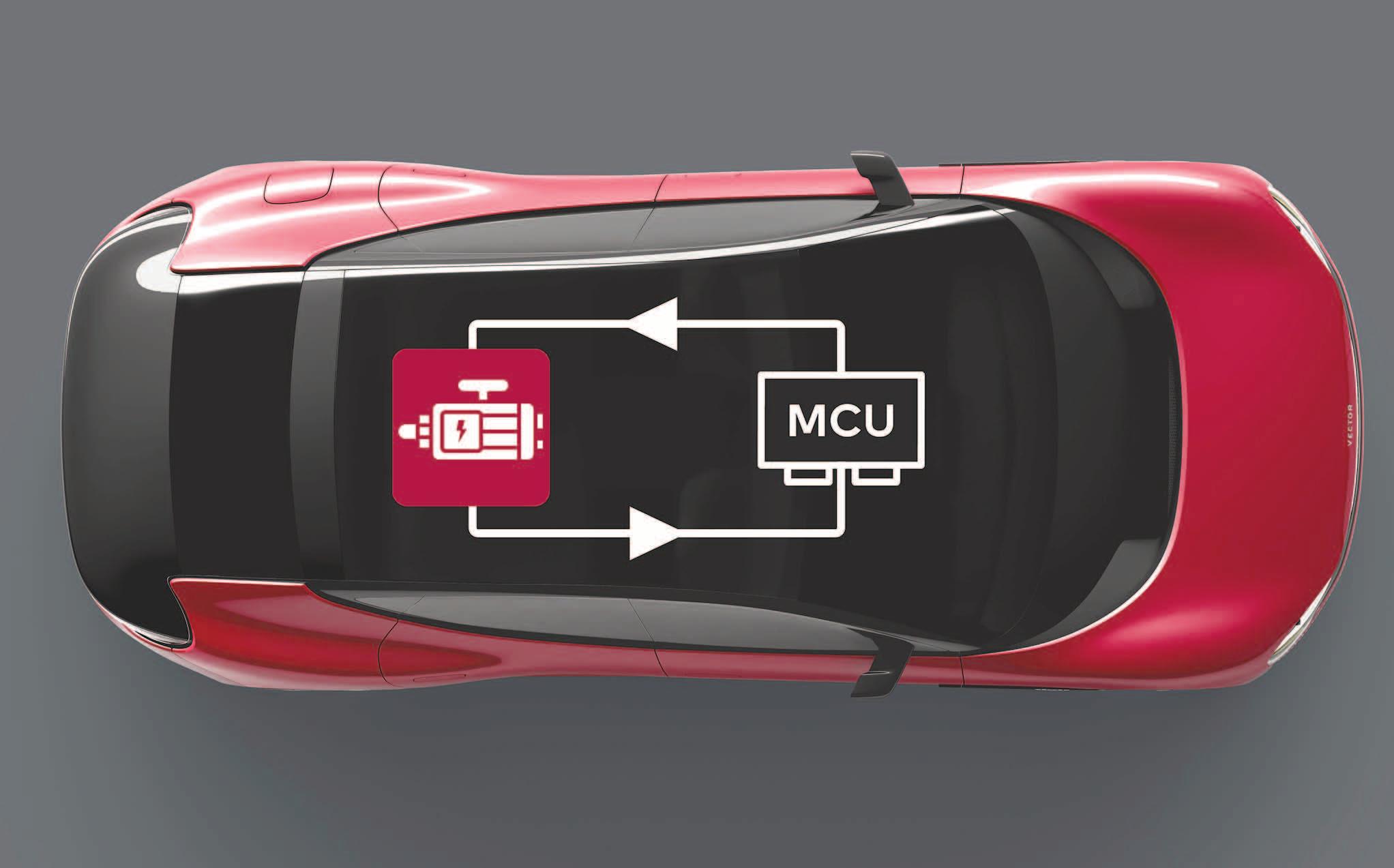
With the new Model Option Electric Motor, Vector has added a powerful function to the CANoe test environment since Release 19. Control units for electric motors (MCUs) can now be tested directly out-of-the-box. The option includes preconfigured physical simulation models of electric motors –for early testing before real components are available.
The Model Option provides ready-to-use physical simulation models for various motor types, such as permanent magnet synchronous motors, brushless DC motors, induction motors, and conventional DC motors. The simulation models close the control loop and thus deliver consistent and realistic input signals to the control unit under test. Since the interface to the MCU operates at the signal level, high currents and voltages are avoided in the test setup. Thanks to high-frequency pulsewidth modulated signals, the model runs on the FPGA of the Vector Multi-IO module VT5838. The test setup enables, for example, validation of motor control under normal operating conditions or with fault injection via CANoe.

The BMI570 provides dependable activity tracking, advanced gesture recognition and accurate head-orientation data for spatial audio. Its robustness under dynamic sports and everyday movements makes it a strong fit for next-generation wearables and hearables.
Responsible innovation and forward-looking architecture
Across all variants, the BMI5 platform meets Bosch Sensortec’s highest ecological standards to date, combining technical performance with responsible innovation. This unified architecture enables device makers to streamline development across product lines, while supporting future edge-AI and ML-enabled enhancements.
■ Bosch Sensortec | www.bosch-sensortec.com

Pre-configured simulation models can be loaded onto the FPGA module with a single click and are immediately ready for use. Parameters can then be easily adjusted in CANoe to match the characteristics of the real motor. For advanced requirements, open models with a Simulink library are available, including additional electrical components such as sensors and inverters for individual model customization.
The CANoe Model Option Electric Motor is designed for developers and test engineers working on electric motor control units for actuators as well as traction motors. For validation in the complete vehicle, the test setup can be extended easily with the virtual test drive using Vector DYNA4. Supporting the optimization and validation of control strategies, the CANoe Model Option Electric Motor helps improve quality and efficiency in the development and testing of electric motors and components.
More information at: www.vector.com/electric-motor
■ Vector | www.vector.com


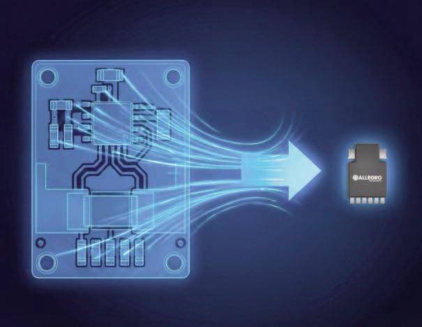
Allegro MicroSystems, Inc. announced the ACS37200, a galvanically isolated current sensor that provides a breakthrough solution to the efficiency and power density challenges in high-current applications. As engineers design increasingly compact and powerful systems for hybrid and battery electric vehicles (HEV/EVs), industrial automation, AI data centers, and solar inverters, the heat and power loss generated by traditional shunt resistors has become a primary design bottleneck. The ACS37200, with its industryleading 50 μΩ conductor resistance, removes this obstacle, enabling designers to build smaller, more efficient, and more reliable power systems.
In a high-current system, every milliohm of resistance matters. A typical 100A design using a 0.5mΩ shunt resistor can waste up to 5 watts of power as pure heat, requiring costly and spaceconsuming heatsinks. The ACS37200’s ultra-low 50 μΩ resistance reduces that power loss to just 0.5 watts - a 90% reduction. This means less energy is wasted and more power is available to drive the vehicle or run the server, directly improving HEV/EV range and lowering data center operating costs. This efficiency gain is a critical enabler for power density. While Allegro’s previous generation of integrated sensors, such as the ACS772, already offered a nearly 7x size reduction over bulky discrete shunt solutions, the new ACS37200, in its compact 100 mm² PSOF package, takes this even further. It is nearly 70% smaller than the ACS772’s CB package, resulting in a total footprint that is 20 times smaller than a traditional shunt solutiona significant 95% reduction in board space. Because the sensor generates minimal heat, designers can eliminate bulky heatsinks, and its integrated architecture removes external isolation components, directly enabling this new level of compactness and higher power density.
■ Allegro MicroSystems | www.allegromicro.com

Renesas Electronics Corporation is expanding its softwaredefined vehicle (SDV) solution offerings centered around the fifth-generation (Gen 5) R-Car family. The latest device in the Gen 5 family, the R-Car X5H is the industry’s first multi-domain automotive system-on-chip (SoC) manufactured with advanced 3nm process technology. It is capable of simultaneously running vehicle functions across advanced driver assistance systems (ADAS), in-vehicle infotainment (IVI), and gateway systems.
Renesas has begun sampling Gen 5 silicon and now offers full evaluation boards and the R-Car Open Access (RoX) Whitebox Software Development Kit (SDK) as part of the next phase of development. Renesas is also driving deeper collaboration with customers and partners to accelerate adoption. At CES 2026, Renesas will showcase AI-powered multi-domain demonstrations of the R-Car X5H in action.
R-Car X5HThe R-Car X5H leverages one of the most advanced process nodes in the industry to offer the highest level of integration, performance and power efficiency, with up to 35 percent lower power consumption than previous 5nm solutions. As AI becomes integral to next-generation SDVs, the SoC delivers powerful central compute targeting multiple automotive domains, with the flexibility to scale AI performance using chiplet extensions. It delivers up to 400 TOPS of AI performance, with chiplets boosting acceleration by four times or more. It also features 4 TFLOPS equivalent* of GPU power for high-end graphics and over 1,000k DMIPS powered by 32 Arm® Cortex®-A720AE CPU cores and six Cortex-R52 lockstep cores with ASIL D support.

Leveraging mixed criticality technology, the SoC executes advanced features in multiple domains without compromising safety.
As hardware and software become more tightly integrated early in development to support complex E/E architectures, Renesas is adding new capabilities to the RoX development platform. RoX dramatically simplifies development by combining all essential hardware, operating systems, software and tools required to rapidly develop next-generation vehicles with seamless software updates.

To accelerate time-to-market, Renesas now offers the RoX Whitebox Software Development Kit (SDK) for the R-Car X5H, an open platform built on Linux, Android, and XEN hypervisor. Additional support for partner OS and solutions is available, including AUTOSAR, EB corbos Linux, QNX, Red Hat and SafeRTOS. Developers can jumpstart development out of the box using the SDK to build ADAS, L3/L4 autonomy, intelligent cockpit, and gateway systems. An integrated stack of AI and ADAS software enables real-time perception and sensor fusion while generative AI and Large Language Models (LLMs) enable intelligent human-machine interaction for next-generation AI cockpits. The SDK integrates production-grade application software stacks from leading partners such as Candera, DSP Concepts, Nullmax, Smart Eye, STRADVISION and ThunderSoft, supporting end-to-end development of modern automotive software architectures and faster time to market.
■ Renesas Electronics Corporation | www.renesas.com
Allegro
Simplifies SiC Power Design for AI Data Centers and EVs with Expanded Power-Thru™ Gate Driver Portfolio
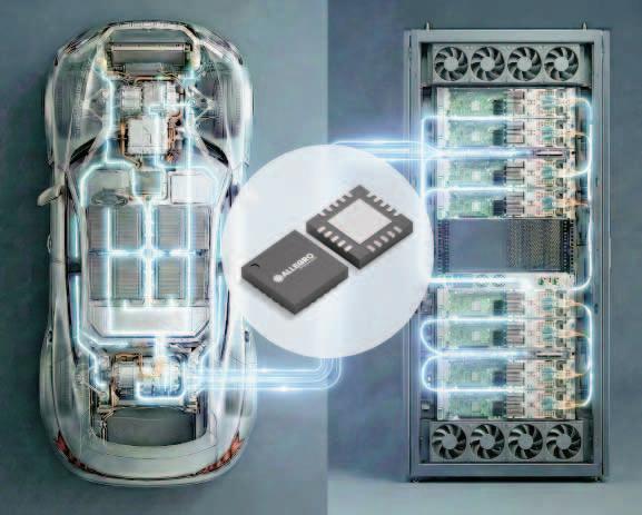
Allegro MicroSystems, Inc. announced the strategic expansion of its Power-Thru™ isolated gate driver portfolio with the launch of the AHV85003/AHV85043 chipset. Joining the flagship AHV85311 integrated solution, this expanded family creates a complete ecosystem for high-voltage silicon carbide (SiC) designs in AI data centers, electric vehicles (EVs), and clean energy systems. The solution simplifies the design challenge in power conversion by eliminating the need for external isolated bias supplies for gate drivers. This innovation delivers the industry’s smallest solution footprint while reducing the bill of materials (BOM) to address the critical challenge of achieving maximum power density, especially in demanding 800V systems.
Allegro’s Power-Thru™ isolated gate drivers integrate signal and power across a single isolation barrier. This breakthrough approach reduces common-mode capacitance in the system by up to 15x, addressing a major source of noise that impacts efficiency. They deliver up to a 20dB improvement in electromagnetic interference (EMI) performance, which boosts overall system efficiency and eliminates countless hours spent by designers resolving noise issues.
In addition to addressing the physics of noise, the expanded Power-Thru portfolio is engineered to resolve critical business challenges. To ensure supply chain resilience, both the new AHV85003/AHV85043 chipset and the existing AHV85311 integrated solution support a multi-source SiC strategy. With selectable gate-to-source voltages (Vgs) of 15V, 18V, and 20V, and adjustable regulated negative voltage, designers can easily swap between SiC FETs from different vendors without redesigning their boards.
Furthermore, the portfolio now offers two distinct implementation paths. The flagship AHV85311 integrated solution, which includes the isolation transformer, provides an all-inone route for accelerating time-to-market. The versatile new AHV85003/AHV85043 chipset empowers designers to optimize for cost and layout by selecting their own external transformer tailored for their specific isolation needs.
■ Allegro MicroSystems | www.allegromicro.com


Edge AI applications utilize computer vision algorithms to detect people, objects, or anomalies such as defects, in real time. Processing images and videos at the edge typically requires a vision AI microprocessor (MPU) that can interface with cameras, run AI models, and often includes a dedicated AI accelerator.
Author:
Rolf Horn, Applications Engineer, DigiKey
Integrating vision AI capabilities into a single device reduces the cost and bulk of using separate components, making
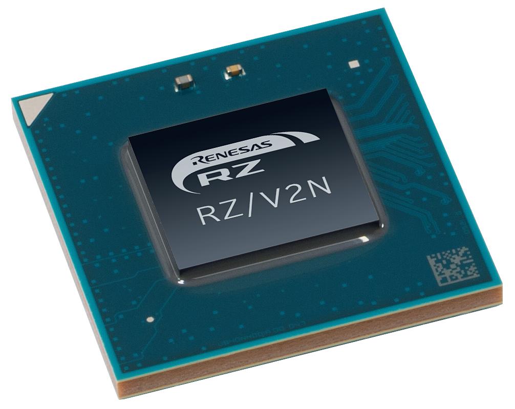
The RZ/V2N (Figure 1) from Renesas Electronics is a vision AI MPU that features low power consumption, high AI inference performance, four Arm® Cortex® A55 CPU cores (1.8 GHz), an Arm Cortex-M33 (200 MHz), and two camera inputs via MIPI connection.
This Renesas MPU is a cost-effective solution for edge applications that require moderate to high AI capabilities at an affordable price point. It is part of the company’s RZ/V series, which aims to deliver a wide range of scalability from smart offices to drones (Figure 2).
Edge AI applications often run in embedded devices, which may be battery-powered or operate on low reserves of energy.
As a result, vision MPUs need to deliver

high inference capabilities while simultaneously using less power than traditional high-performance computing devices. The ideal vision AI MPU balances performance, power efficiency, integration, ease of development, and security.
An overview of some of the key features in selecting an MPU are:
• Inference performance : The RZ/V2N delivers up to 15 TOPS using its integrated DRP-AI3 accelerator, making it suitable for mid-range applications such as smart cameras, industrial inspection, and edge robotics. While some high-performance systems, such as collaborative robots and autonomous drones may require 80 to 100 TOPS, many edge AI applications operate well with 1 to 15 TOPS, depending on their complexity.
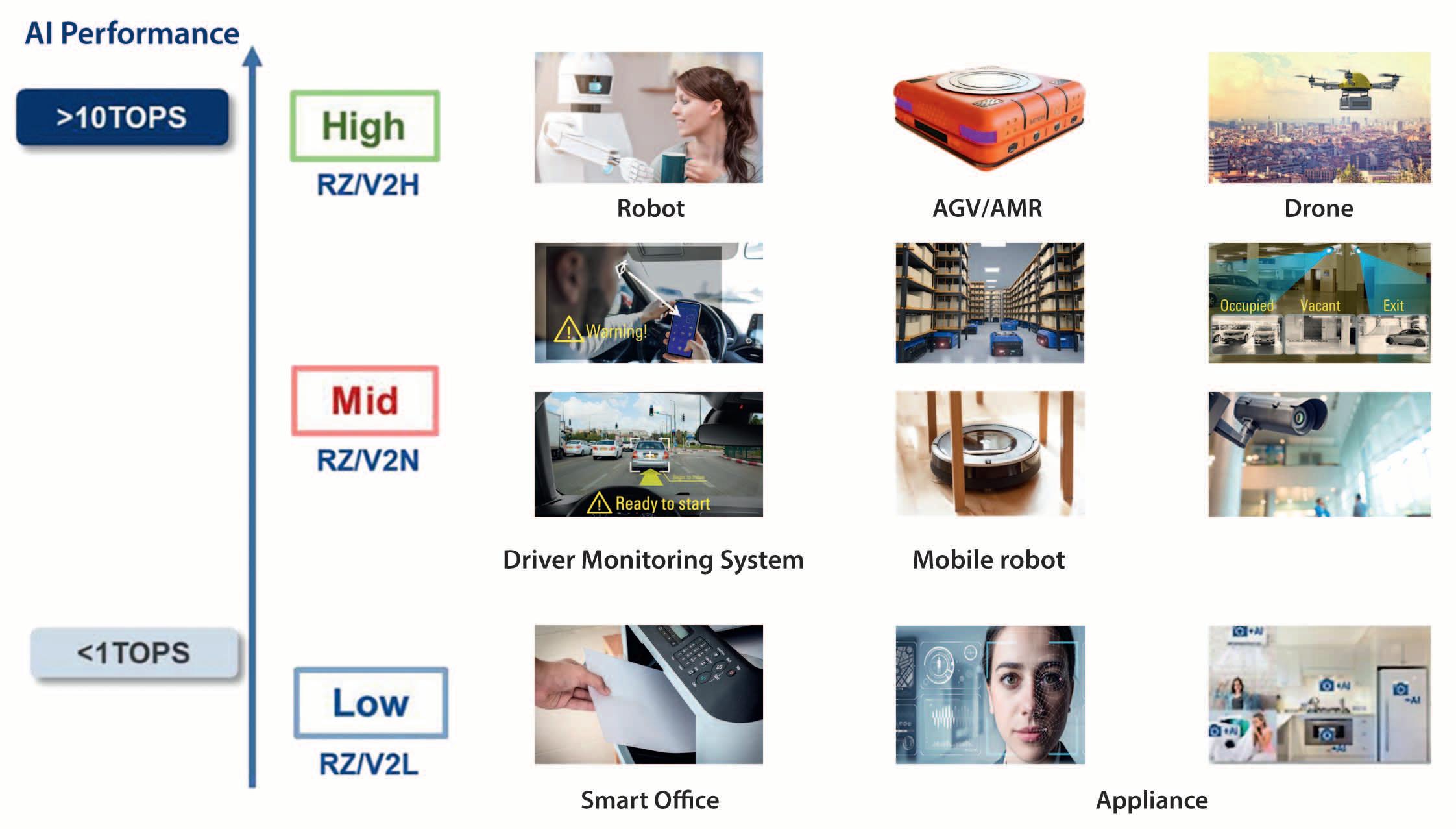
Figure 2 Positioned as a mid-range offering in the RZ/V line, the RZ/V2N enables applications such as mobile robots for home use and driver monitoring systems.
TOPS per watt (TOPS/W) defines the product’s efficiency, which is a measure of how many operations it can perform per second per watt.
Although TOPS gives a baseline indication of performance, actual inference speed can be significantly improved with the inclusion of a dedicated AI accelerator, which offloads vision AI workloads that rely on intensive matrix and tensor computations. This allows systems to operate faster and more efficiently, with fewer clock cycles and lower power draw.
• Low-power operation: Many edge devices run on batteries or within strict thermal limits. Vision MPUs designed for edge AI often include dynamic voltage and frequency scaling (DVFS), which adjusts power use based on workload demands. Combined with techniques like neural network pruning – which compress model size and reduce unnecessary calculations – DVFS helps achieve a higher TOPS/W ratio, improving both runtime and battery life.
The DRP-AI3 accelerator helps avoid the need for power-hungry GPUs, contributing to higher TOPS/W at the edge.
• On-chip image processing : Vision microprocessors with optional built-in image signal processors (ISPs) can per-


form routine image cleaning tasks, such as black level correction, color correction, cropping, and shading correction. In security or surveillance applications, the ISP can also pre-filter frames. For example, in a continuous video stream, the system may discard static frames and only send frames with motion or activity (e.g., intruder detection) to the AI processor, reducing unnecessary inference and saving power.
• On-chip memory: Memory is also an important factor for performance and efficiency. Keeping data local avoids the latency and power cost of accessing external memory, which can be significant during real-time AI inference. With 1.5 MB of on-chip SRAM and support for LPDDR4X memory, the RZ/V2N balances internal processing speed with expandable memory options.
• Accelerating AI deployment: AI toolkits and evaluation boards that include preprogrammed applications and interfaces can help developers to quickly prototype and deploy vision AI applications. In addition, the MPU should be able to support standard AI model formats. The RZ/V2N is compatible with standard model formats, such as ONNX and TensorFlow Lite.


• Security: In edge environments, every sensor or endpoint can represent a potential attack vector. Therefore, it's important for vision MPUs to be able to support builtin security features such as secure boot and encrypted data paths. The RZ/V2N includes secure boot and hardware-level encryption features, and it leverages Arm TrustZone for isolating secure operations, helping protect both model integrity and sensitive input data.
AI DESIGN-FRIENDLY FEATURES OF THE RZ/V2N MPU
Renesas’ proprietary AI accelerator, the DRP-AI3 (Dynamically Reconfigurable Processor), is rated at 10 TOPS/W but can be enhanced up to 15 TOPS/W with advanced pruning, which compresses the size of the models that the system must process. This can eliminate the need for a separate graphics processing unit (GPU) or field-programmable gate array (FPGA). The RZ/V2N measures just 15 sq mm, which makes it a good option for compact devices. Combining a quad-core CPU, a dedicated AI accelerator, and support for dual camera inputs into a single device opens new opportunities for designers to integrate vision AI into applications such as smart cameras, security devices, robots, and even consumer appliances.
The MPU operates on low power, which reduces the amount of heat generated, eliminating the need for additional cooling systems and fans, and thereby reducing the size and cost of embedded systems. With the ability to accommodate two cameras, it enables applications to capture double-angle images and improve spatial recognition.
• AI Accelerator: The Renesas DRP-A13 dedicated AI engine enables high-speed AI inference processing that achieves the low power and flexibility required by endpoints.
• Video and graphics: Optional graphics processing unit (GPU) and ISP that help process images and render graphics more efficiently.
One system can perform multiple opera tions, such as simultaneously counting cars in a parking lot and recognizing license plates.
THE ARCHITECTURE OF THE RZ/V2N MPU
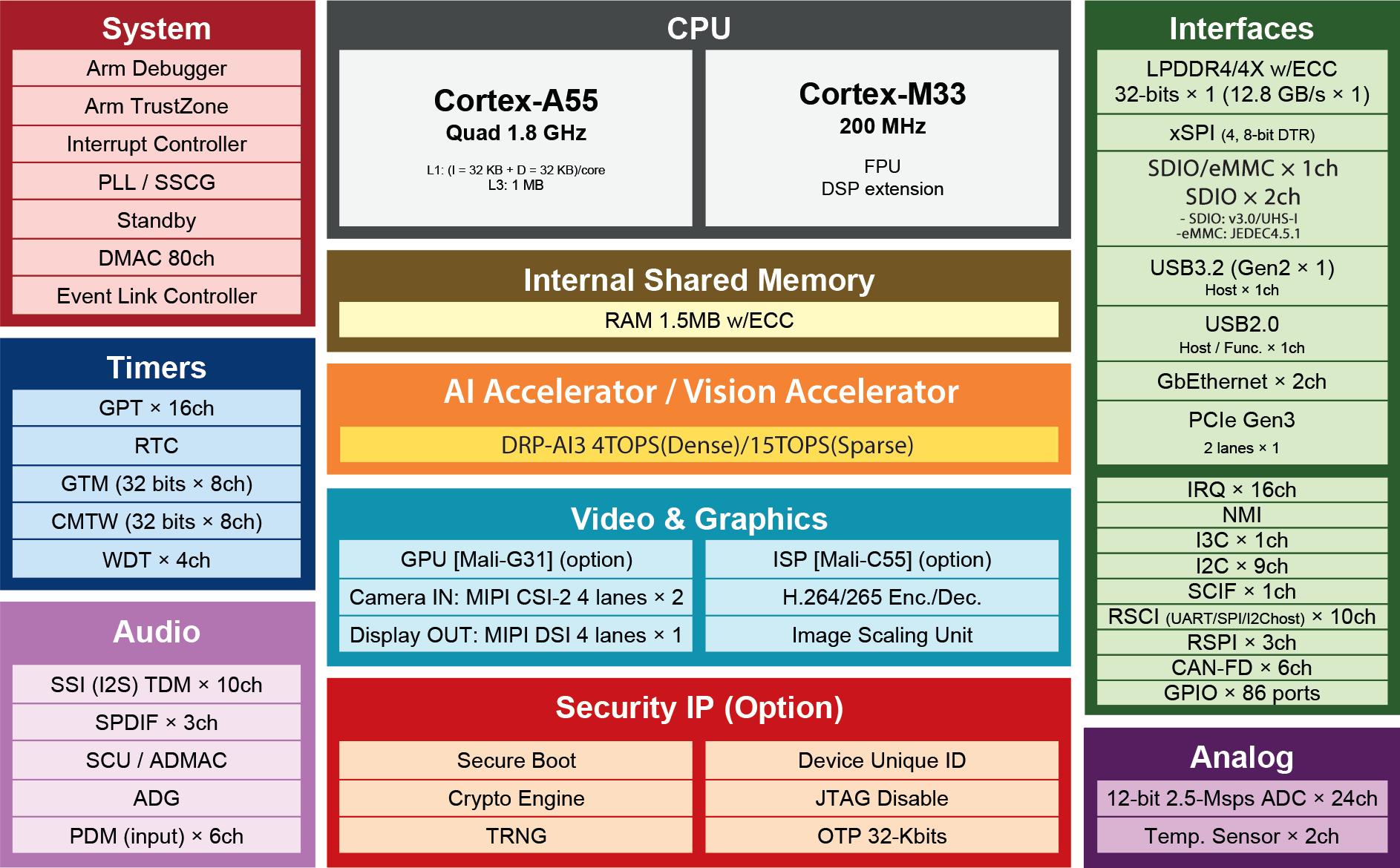
The RZ/V2N MPU provides a comprehen sive array of features and functions designed for creating mid-range AI market applications that require high-perfor mance AI at an affordable price (Figure 3).
Some of the key features include:
• Central processing unit (CPU) : The hybrid architecture features the CortexA55 Quad 1.8 GHz, a high-performance CPU, and the Cortex-M33 200 MHz, a lowpower core designed for real-time con trol and safety-related tasks.
• Internal shared memory: 1.5 MB RAM for on-chip memory with error-correcting code (ECC), which helps data integrity. ECC algorithms detect and correct errors in data, both in storage and transmission. The 1.5 MB on-chip memory enables AI algorithms to run quickly, and the RZ/V2N also has an interface for external DDR memory that can be added if more memory is needed.
are among the many interfaces that can connect to the vision microprocessor module.
• Analog block: A 12-bit analog-to-digital converter (ADC) eliminates the need for separate ADCs in control systems or monitoring applications.
Renesas also offers the RTK0EF0186C03000BJ evaluation board kit for the RZ/V2N to enable designers to prototype and evaluate vision AI applications (Figure 4).
Designers can also access AI applications covering more than 50 use cases in the company's AI applications and AI SDK on GitHub.
The RZ/V2N from Renesas is a good fit for mid-range edge AI applications that need to deliver data-driven information with reduced latency at high speeds. Its compact size and ability to meet inference demands while running on low power, make it suitable for a wide range
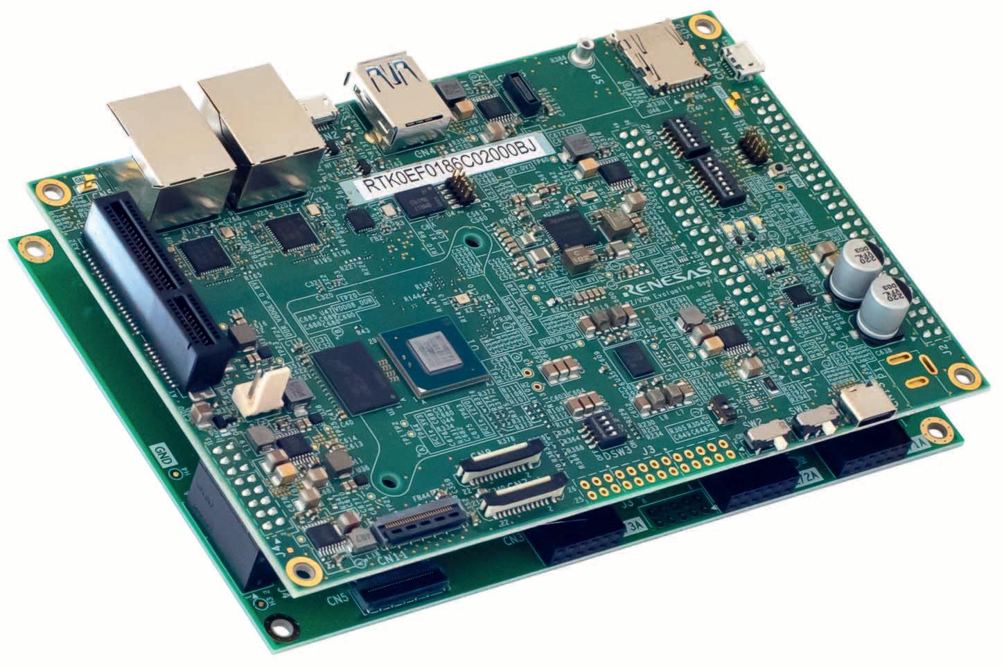
The evaluation board kit for the RZ/V2N includes a CPU board, expansion board, and two sub-boards, along with an AI SDK.
• Timers: Timers support real-time operations, which are essential for motor control and other automation applications.
• Audio block: Ideal for multi-channel audio applications, such as smart speakers and infotainment systems.
• Interfaces: High-speed memory interfaces and high-bandwidth peripherals
■ DigiKey www.digikey.com

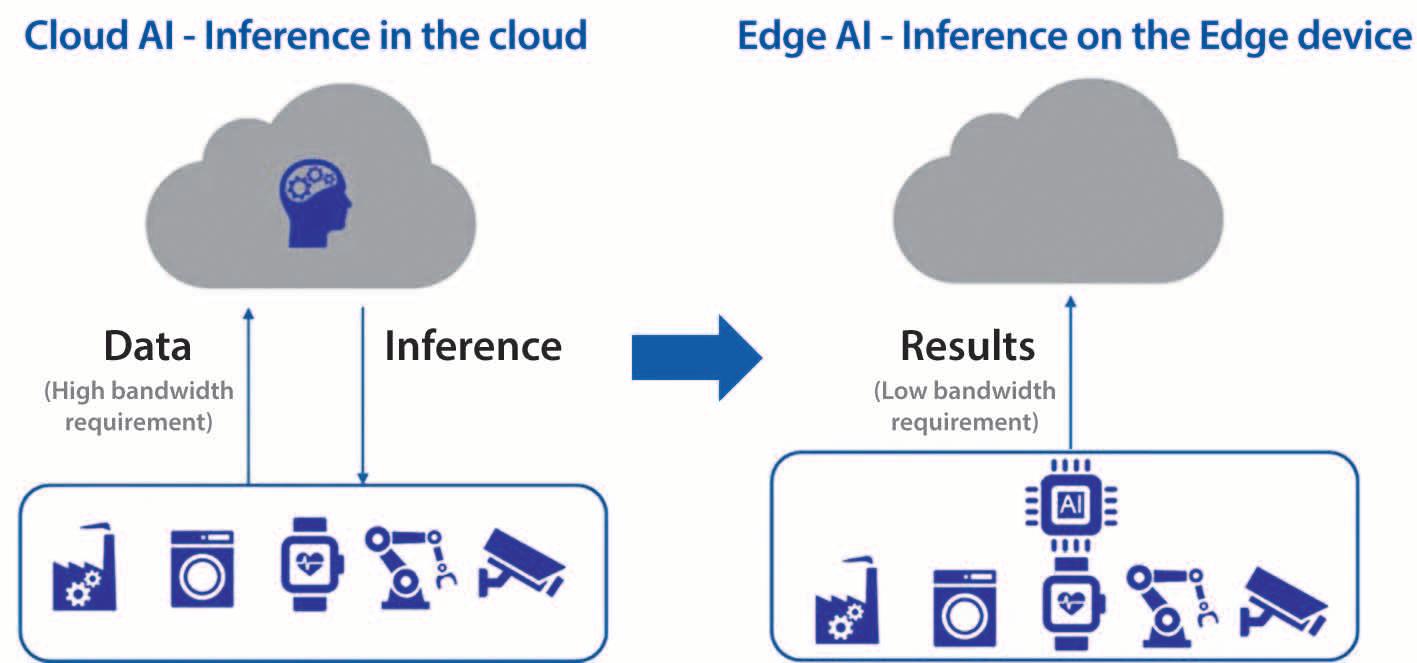
There has been a paradigm shift in the AI market. Previously, AI processing was done mainly in the cloud. End point devices gathered data from sensors and sent it to the cloud for inference processing and decision making and results were sent back to the end point devices. This approach suffered from larger latency, higher power, security risks and required huge bandwidth for transmission of data to the cloud. IDC estimates that 79.4ZB of data will be sent from IoT devices to the cloud in 2025.

Author: Kavita Char, Principal Product Marketing Manager Renesas Electronics
For these reasons, there is an increasing movement towards AI inference at the Edge that enables fast real-time responses and increased data privacy and security, while avoiding the latency and costs associated with the cloud connection. This also lowers power consumption, making it suitable for battery powered IoT and consumer applications. AI at the edge, therefore, provides advantages of autonomy, lower latency, lower power, lower costs with lower bandwidth to cloud and higher security, all of which make it attractive for new and emerging applications.
There are a number of solutions addressing the Edge AI market. The choice between an MPU and an MCU for AI implementation depends on the specific application requirements. MPUs are suitable for complex applications requiring high processing power, while MCUs are ideal for low-power, cost-sensitive applications where real-time processing and energy efficiency are crucial.
Neural network processing requires various linear algebra operations, dot products and


a series of fast, parallel matrix multiplications, convolutions and transpositions. This demands higher computational power in processors. MCU manufacturers are now introducing devices that include advanced CPU cores with enhancements to support DSP and AI/ML operations, such as Helium vector extensions on the Arm Cortex-M85 core. MCU manufacturers are also integrating a Neural Processing Unit (NPU) on the MCU, designed to accelerate AI inference tasks.
1 Higher AI/ML processing performance
An NPU has dedicated hardware to execute core operations of neural network models, such as matrix multiplications and convolutions, more efficiently and with lower latency than the CPU core. NPUs are optimized for lower precision arithmetic (8/4bit integer) used in AI models, which reduces complexity, memory use and power consumption without reducing inference accuracy.
2 Efficient system partitioning NPUs handle the AI tasks and free up the main CPU to perform pre- and post-processing of AI data and execute application
code and other system tasks such security, sensor interfaces and communications, resulting in system performance improvements.
3. Lower power consumption
The NPU can process models with much lower power consumption than the CPU core, making them especially suited for edge devices where low power is crucial.
4 Higher security NPUs allow inference processing and decision making on the edge device minimizing data transmission to the cloud, ensuring data privacy and integrity.
What is needed to make low power Edge AI a reality is a fully integrated, high-performance AI accelerated MCU that enables highly secure, low power inference capability with faster real-time responses.
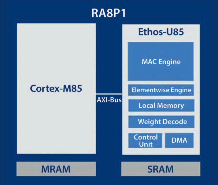
The RA8P1 MCUs are Renesas’ first AIaccelerated single and dual-core MCUs and are built on the advanced TSMC 22nmULL process, combining the highest performance Arm® Cortex®-M85 (CM85) and Cortex-M33 (CM33) CPU cores with the Arm EthosTM-U55 neural network processor (NPU) to deliver a huge uplift in AI/ML, DSP and scalar performance – ideal for Edge AI and IoT applications.
by enabling higher processing power, efficient task partitioning between the two cores and improved real-time performance and power efficiency. In addition, advanced security, immutable memory and TrustZone are built in to enable truly secure AI applications.
The Arm Ethos-U55 NPU embedded in the RA8P1, is a dedicated processor optimized to execute core operations of neural network models, such as matrix multiplications and convolutions, more efficiently and with lower power consumption than the CPU core.
The NPU is designed to work seamlessly with Cortex-M cores. It offloads the CPU core and supports all the operators used in CNNs and RNNs.
It supports 8bit weights and 8/16bit activations and uses system SRAM and nonvolatile memory for its operation via two 64bit AXI master interfaces. It uses weight compression and de-compression to improve inference speed and reduce memory needs.
It also supports fallback mode – the operators not supported by the NPU fall back to the main Cortex-M CPU core, accelerated in software using CMSIS-NN.
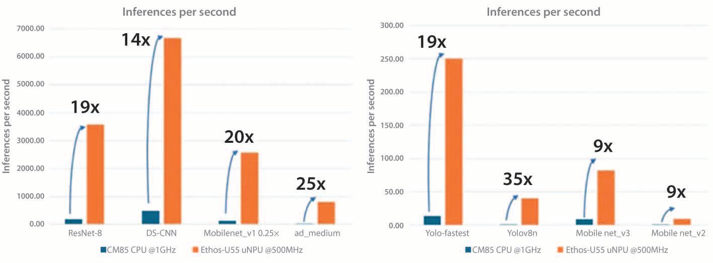
These highly integrated MCUs deliver an unprecedented 7300+ CoreMarks raw performance, 256 GOPS of AI performance and together with large memory and a rich peripheral set, drive demanding Voice, Vision AI and Real-Time Analytics applications, providing orders of magnitude higher processing performance than a CPU core alone.
Dual-core RA8P1 MCUs significantly enhance the performance of AI applications


Ethos-U55 supports most commonly used neural network models such as DSCNN, ResNet, MobileNet, Inception, Wav2Letter etc.
Renesas has successfully demonstrated the inference performance uplift with RA8P1 MCUs using Ethos-U55 for inference processing, with a few AI/ML use cases, showing a significant performance uplift with the Ethos-U55 NPU as compared to the CPU core.


MODELS USED:
• Image classification – ResNet8, MobileNet v2, MobileNet v3
• Keyword Spotting – DS-CNN
• Visual wake words – MobileNet v1
• Object Detection – Yolo_fastest, Yolov8N
• Anomaly Detection – ad_medium
FASTER APPLICATION
DEVELOPMENT WITH RUHMI FRAMEWORK
The RA8P1 AI solution features the RUHMI Framework, Renesas’ first comprehensive AI development environment for MCUs and MPUs, integrated into Renesas e2 studio IDE to optimize and deploy highly optimized neural network models in a framework agnostic manner. RUHMI enables model optimization, quantization and conversion to an MCU friendly format. It provides all the necessary tools, APIs, code-generator, and runtime needed to deploy a pre-trained model on the RA8P1. Native support for commonly used ML frameworks TensorFlow Lite, Pytorch and ONNX is included, along with ready to use application examples and models optimized for RA8P1.
TYPICAL AI WORKFLOW WITH RUHMI:
1 Model optimization and compilation (Offline): A pre-trained AI model is input via commonly used frameworks such as Tensorflow Lite, quantized to an Int8 intermediate format and optimized for execution on the NPU or CPU core. The model is then compiled to an MCU friendly format (typically *.c/*.h) that can be executed by the NPU.
2 Data Input and Pre-processing: Raw input data (image from a camera, audio from a microphone) is captured by the MCU. This data is then pre-processed by the CPU to scale and format it for input to the AI model. ©
3. Execution on the NPU: The CPU core sends the pre-processed input data and the compiled AI model's command stream to the NPU for execution.
• Real-time Analytics – Anomaly detection, vibration analysis, predictive maintenance
labeled images, until the model’s prediction accuracy is very high.
The NPU reads the command stream and using the input data and model weights (typically stored in local memory), processes each layer of the neural network, passing intermediate results to adjacent layers of the network.
• Multimodal applications – Smart HMI with voice and vision capability, enhanced surveillance cameras, robotics with visual and auditory inputs for environment sensing and interaction
This pre-trained model can be deployed on the RA8P1 MCU. For inferencing, a new input image is fed into the model and goes through the layers of the trained network.
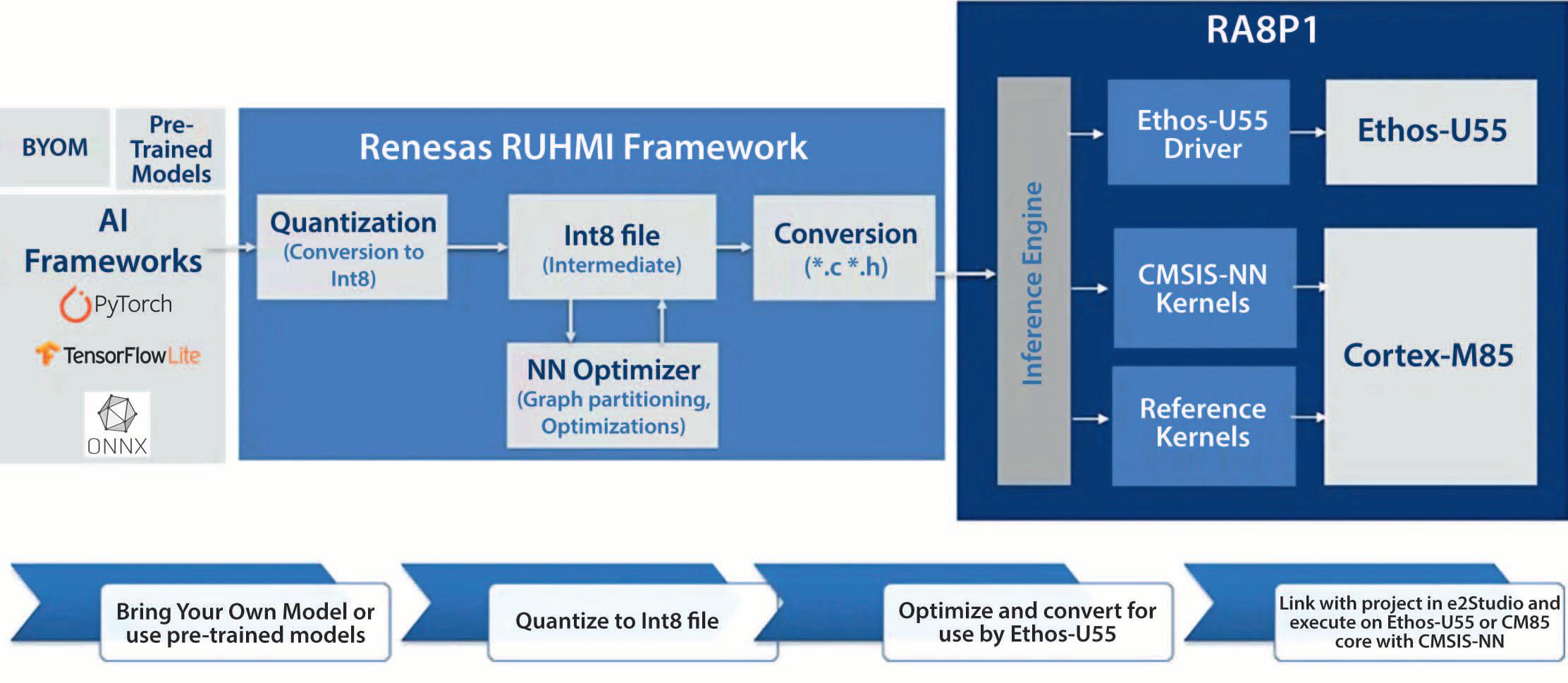
4 Output and Post-processing: Once the NPU has processed all layers of the neural network, it outputs the inference results (e.g., object bounding box coordinates and classification or a "wake word detected" signal) back to the main CPU, which can then perform any necessary post-processing and action (e.g., overlaying bounding boxes on an image, triggering an action, sending data to the cloud).
AI APPLICATIONS ENABLED BY RA8P1
With its high inference performance, low power consumption and real-time processing capability, the RA8P1 is ideal for a wide range of AI applications across various market segments, such as:
• Voice AI – Keyword Spotting, voice recognition, speech recognition, speaker identification
• Vision AI – Object detection, image classification, gesture recognition, face recognition, image analysis, driver/ vehicle monitoring
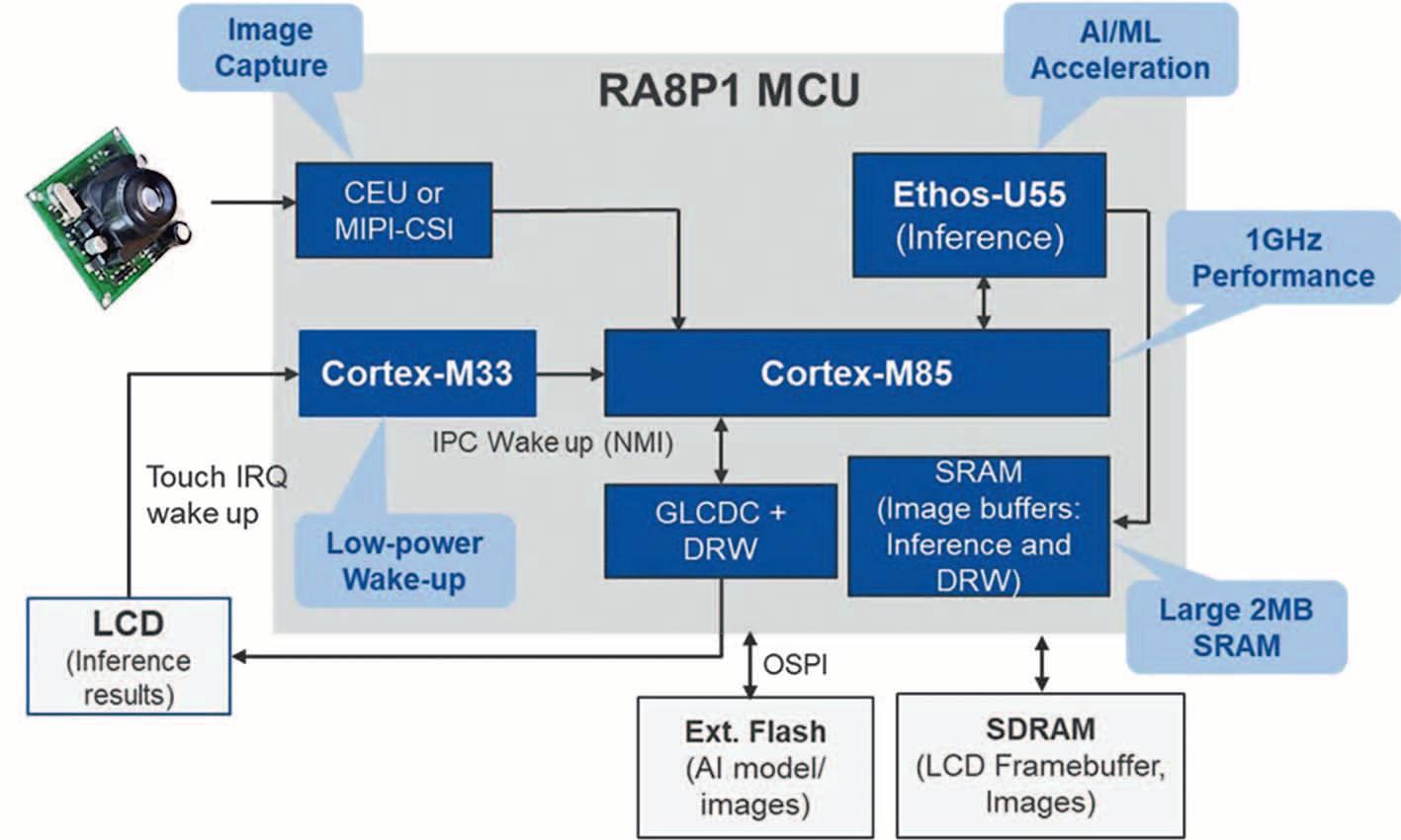
Image Classification System Block Diagram.
In the next section, we will see two examples of AI implementations on RA8P1.
APPLICATION EXAMPLE 1:
IMAGE CLASSIFICATION ON RA8P1
Figure 5 shows an Image Classification AI application that analyzes an input image and assigns it a pre-assigned label or category. The neural network model is trained iteratively on a vast dataset of
The output layer then provides the probabilistic distribution across all categories and the category with the highest probability is assigned as the image’s label. This output data (image label and accuracy) can then be sent to the display or to the cloud.
In our implementation, we see a 33x improvement in inference speed with the Ethos-U55 in comparison to using the
CPU core, and a power consumption of 62mA running inferences at 1000fps (including external memory accesses).
The average current consumption measured while running all 4 models was 86mA.

Image classification can be used in diverse applications:
• Security – identifying weapons, people recognition, anomaly detection
• Retail – creating product catalogs by category, inventory management
• Agriculture – identifying crop disease, classification of plants
• Smart Cities – identifying traffic lights/signs and pedestrians
• Smart appliances – identifying objects inside refrigerator
APPLICATION EXAMPLE 2: DRIVER MONITORING SYSTEM ON RA8P1
This application shows the Nota-ai Driver Monitoring System (DMS) which is an in-cabin safety solution to enhance road safety for all aspects of vehicle travel. The Nota-ai DMS runs multiple models to detect unregistered drivers, driver drowsiness, cell phone usage, and driver distractions like smoking.
Using the RA8P1, we see a 4x-24x increase in inference performance for the four models being used in this application – face detection, face landmark, eye landmark and phone detection.
The DMS finds application in dashboard cameras, vehicle data recorders, and driver monitoring systems.
BOTH THESE VISION AI APPLICATIONS MAKE OPTIMAL USE OF THE RESOURCES ON THE RA8P1 MCU
1 Efficient input image acquisition via the image sensor
The RA8P1 includes a MIPI CSI-2 interface with an image scaling unit or the 16bit CEU parallel camera interface for capturing raw image input data.
2 High performance inference processing with the Ethos-U55 NPU
The Ethos-U55 AI accelerator receives processed images from the MIPI CSI-2 or CEU camera interface and processes complex AI models more efficiently and with lower power consumption than the CPU core.
3. Faster application processing with Arm Cortex-M85 and Cortex-M33 CPU cores
- The high performance 1GHz CM85 core with Arm Helium vector extensions is used for pre- and post-processing of the input data and the inference results. Operators not supported by the Ethos-U55 can be executed by the CM85 core in fallback

mode. With the inference processing offloaded to the NPU, the CM85 CPU can be used fully for compute intensive application code.
- The 250MHz Cortex-M33 core on dualcore RA8P1 MCUs can be used for low power wake-up and housekeeping tasks.
4. Efficient storage of images, model weights and activations with on-chip memory and memory interfaces
- The on-chip 1MB MRAM and 2 MB SRAM are crucial for storing AI model weights, images and intermediate results.
- High-throughput external memory interfaces (OSPI with XIP and Decryption on the fly and 32bit SDRAM) can be used for larger models.
5 Advanced Graphics peripherals for graphics processing and HMI
The Graphics LCD controller (with parallel or MIPI DSI interfaces) and 2D graphics engine can be used for rendering images and inference results to the LCD display.
6 Flexible Connectivity options
Several connectivity options exist to transmit inference results, images or alerts/ notifications either to local devices or to the cloud, for storage or analysis
Edge AI applications benefit greatly from the use of AI accelerated MCUs. They enable applications where real-time performance, low power and security are critical concerns. The addition of the NPU to low power MCUs has been a transformational change in the AI solutions landscape. The new RA8P1 MCUs drastically reduce latency, enable data privacy and minimize power consumption, making them ideal for battery-powered applications. The entire development is supported by Renesas’ comprehensive RUHMI Framework, which helps developers optimize and deploy their AI models efficiently on the RA8P1 hardware.
For more information, visit: www.renesas.com/en/products/ra8p1
■ Renesas
www.renesas.com


Mouser Electronics announces a global distribution agreement with Telit Cinterion, an end-to-end IoT solutions enabler, for their industrial-grade cellular, wireless communication, and positioning modules for IoT and IIoT solutions.
“Mouser is pleased to add Telit Cinterion to our global line card,” said Kristin Schuetter, Mouser Senior Vice President of Products. “Their innovative, high-performance IoT portfolio of products will greatly benefit design engineers and manufacturers. We are committed to serving the design needs of our customers and look forward to a successful partnership.”
“We’re excited to join Mouser’s list of global manufacturer partners,” commented Jitender Vohra, VP of Global Channel Sales for Telit Cinterion. “The agreement provides us with an incredible opportunity to bring our
industry-leading connectivity and location solutions to Mouser’s extensive customer base. We look forward to collaborating with their team as we support customers seeking to develop the next generation of IoT and IIoT applications.”
LTE Cat 1bis Modules for Reliable Global IoT Connectivity
Among the product offerings are Telit Cinterion’s LE910Q1 and LE910R1 LTE Cat 1bis modules, developed specifically to support IoT applications, including a wide range of value-oriented applications that require reliable data speed and global coverage.
Cat 1bis uses existing LTE networks but operates with a single antenna, enabling more compact and simpler designs. These modules are ideal for asset tracking, vehicle telematics, and remote monitoring applications.
LTE-M and NB-IoT Modules for Low-Power Wide-Area Applications
The ME310G1-WW and ME910G1-WW cellular LPWA LTE-M and NB-IoT modules are designed for IoT applications that require minimal data transmission, improved power efficiency and superior coverage quality. The ME910G1 series is ideal for global IoT applications such as smart metering, security and surveillance, point of sale, health monitoring, fleet management, and asset tracking. While the ME310G1 series smaller form factor is ideal for wearable medical devices, fitness trackers, industrial sensors, and many other mass-production, mass-deployed applications.
The WE310x modules, available at Mouser, are fully-integrated Wi-Fi®/Bluetooth® Low Energy (LE) solutions designed to provide an easy, cost-effective way for manufacturers to add wireless connectivity to their products. The WE310x modules are well-suited for developers with RF expertise or for those seeking faster time to market, as they greatly reduce design time and remove the burden of testing and certification. The modules come in several variants, with both integrated antennas and provisioning for external antennas for design flexibility.
Sub-6 Cellular Data Cards for Enterprise and Industrial IoT
The FN990A40 and FN990A28 data cards feature sub-6 only technology with LTE, WCDMA, and GNSS support. These data cards lay the foundation for businesses worldwide to futureproof IoT, enterprise applications, and video while leveraging the benefits of 5G and Gigabit LTE. The FN990A40 data card is targeting high-tier market needs with the FN990A28 data card is suitable for mid-tier market needs. Both cards are offered in the industry standard M.2 (NGFF) form factor.
To learn more about Telit Cinterion, visit https://eu.mouser.com/manufacturer/telit -cinterion
For more Mouser news and our latest new product introductions, visit https://eu.mouser.com/newsroom
■ Mouser Electronics www.mouser.com

Rochester Electronics takes a closer look at the recent tightening in semiconductor supply, outlining the challenges faced by manufacturers and the practical steps needed to build a more robust and reliable supply chain.
The semiconductor industry underpins modern technology, powering everything from automotive systems to medical devices. Yet recent developments highlight how vulnerable global supply chains remain. Inventory shortages for critical components – such as diodes, transistors, and MOSFETs – have cascaded across multiple sectors, resulting in production delays and increased operational costs.
According to Z2Data, inventories of Nexperia’s most critical components fell by 30–50% among authorised distributors in just five weeks, with no signs of near-term recovery. These devices are essential across automotive, industrial, and consumer applications. When supply becomes unstable, production halts, planning becomes uncertain, and OEMs are forced to scramble for alternatives. This shortage is not confined to the automotive sector. Aerospace systems, industrial controls, and medical devices also depend heavily on these parts. Many devices are soldered into assemblies requiring extensive testing and qualification, meaning that substituting components is neither quick nor simple.
Multiple factors have contributed to this tightening of supply:
• Geopolitical tensions: Export controls and regulatory restrictions disrupted manufacturing and logistics flows.
• Single-source dependencies: Heavy reliance on specific suppliers amplified the impact of shortages.

• Just-in-time inventory practices: While efficient during stable periods, these leave virtually no buffer during times of crisis. These dynamics demonstrate how quickly even well-established supply chains can be disrupted by external forces.
When authorised stock becomes scarce, some manufacturers turn to the grey market. This introduces risks such as counterfeit, sub-standard, or non-compliant components – all of which can jeopardise safety, reliability, and brand integrity. In industries where quality is critical, the consequences can be severe.
Manufacturers can strengthen supply chain resilience through proactive measures:
1. Maintain authorised inventory: Work only with distributors who guarantee full traceability and compliance.
2. Diversify sourcing: Avoid over-reliance on any single supplier, region, or manufacturing node.
3. Plan for lifecycle management: Anticipate obsolescence and secure longterm supply agreements.


4. Leverage market intelligence: Use realtime data to forecast demand and identify potential vulnerabilities before they escalate.
Through its authorised partnership with Nexperia, Rochester Electronics secured 2.9 billion Nexperia devices before any production concerns were announced –ensuring uninterrupted availability for customers. Every device is 100% authorised, traceable, and guaranteed. Rochester also partners with leading manufacturers such as onsemi, Texas Instruments, and STMicroelectronics to provide fully authorised alternatives when needed. This strategic foresight demonstrates how trusted partnerships and early action can shield manufacturers from market volatility and protect long-term supply continuity.
The recent inventory challenges serve as a clear reminder: supply chain resilience is not built overnight. It requires planning, diversification, and strong relationships with authorised partners. By prioritising authorised sourcing, investing in lifecycle strategies, and leveraging strong market intelligence, manufacturers can navigate uncertainty with confidence – safeguarding production and protecting their customers.
■ Rochester Electronics www.rocelec.com


Mouser Electronics announces its comprehensive power management resource centre. With the proliferation of compact, high-performance, and battery-operated devices, power management design is critical to achieving optimal performance. By leveraging new advancements in power management, such as smart grid management technology, DC microgrids can enhance energy efficiency and power quality. Their native DC architecture provides seamless integration with DC loads and renewable energy systems, such as EV charging infrastructure. Another method of power management is energy harvesting, where improved conversion efficiency in solar, motion, and thermal harvesting techniques extends battery life or even enables completely battery-free operation.
For chip-level power and performance, modern embedded systems today utilise configurable logic blocks (CLBs). CLBs enable hardware-based functions, such as timing control and power sequencing, resulting in faster response times, reduced CPU load, and lower power consumption. Together, these advancements create a balanced system where power is generated, distributed, and consumed with maximum efficiency, fundamentally improving power management in electronics.
Mouser’s technical team and trusted manufacturing partners tailor the resource center content to provide a trusted source of articles, blogs, eBooks, and new products from top manufacturers for power management. The hub also offers infographics on battery energy storage systems (BESS), helping professionals understand the system complexities and how to select the best-suited components. For engineers looking to stay ahead of the accelerating pace of advanced power management, the resource centre serves as a valuable resource.
Advanced power management approaches for energy-efficient electronics
Mouser stocks the industry’s widest selection of semiconductors and electronic components, including the newest products and solutions for power management applications. Here are a few examples:
• The AEM00300 ambient energy manager battery charger by e-peas is an integrated energy management circuit that extracts DC power from an ambient energy harvesting source. The battery charger PMIC extends battery life and can eliminate the primary energy storage element in many applications.
• The MCP16701 PMIC from Microchip Technology integrates eight DC-DC Buck regulators, four 300mA LDOs, and one LDO
controller. The PMIC supports Microchip eMPUs with dynamic voltage scaling and high-performance mode, as well as PIC64GX, PolarFire FPGAs, and PolarFire SoCs.
• The xG22-EK8200A energy harvesting explorer kit from Silicon Labs is an excellent starting point for exploring and evaluating various energy harvesting solutions with Silicon Labs’ Multiprotocol Wireless SoC. This comprehensive kit supports assessments of different energy sources for both pulsed and continuous power supply applications, accommodating single or dual sources.
• The MP8853 synchronous step-down converters by Monolithic Power Systems (MPS) are high-efficiency, wide-input-voltage-range devices that deliver up to 4A of continuous output current. These fully integrated converters offer excellent load/line regulation.
To learn more, visit: https://resources.mouser.com/powermanagement
For more Mouser news and our latest new product introductions, visit https://eu.mouser.com/newsroom
■ Mouser Electronics www.mouser.com


Ambarella, Inc., an edge AI semiconductor company, announced during CES the launch of its Ambarella Developer Zone. Located at developer.ambarella.com, the DevZone is designed to help Ambarella’s growing ecosystem of partners learn, build and deploy edge AI applications on a variety of edge systems with greater speed and clarity. It provides a collection of optimized models, along with low-code and no-code agentic blueprints, to enable the rapid development of edge AI applications on Ambarella’s large portfolio of purpose-built edge AI systems-on-chip (SoCs) with Cooper development software.
A Unified Developer Hub for Building and Deploying Edge AI Applications
As AI workloads increasingly move towards hybrid edge/cloud architectures, partners need faster, more scalable ways to develop products and services with Ambarella’s full-stack edge AI platform. The DevZone consolidates essential tools, documentation, models and community resources into a single destination, enabling system integrators, distributors, module builders, independent software vendor (ISVs) and other leading global ecosystem partners to engage, prototype and accelerate edge AI solutions for a wide range of vertical industry segments.


The DevZone brings the full breadth of Ambarella’s development resources together in one cohesive environment, including:
• Cooper™ Model Garden: A growing repository of validated, optimized models ready for testing and validation
• Learning & Onboarding Library: White papers, blogs, tutorials and sample applications to help users get started immediately
• Agentic Blueprints: Low-code and no-code templates that enable the rapid design of multi-agent systems through unique, next-generation agentic workflows
Together, these elements create a more intuitive, efficient development experience that helps teams build and validate models rapidly for broader markets. Through its DevZone, Ambarella is strengthening support for ecosystem partners by expanding access to parts of its software stack through agentic interfaces, sample workflows and development resources. This unified entry point makes it easier for ecosystem partners to evaluate Ambarella’s technology, integrate more efficiently and bring solutions to market faster.
This new AI developer zone is positioning the company to build on its leadership in


edge endpoints—with more than 39 million edge AI SoCs shipped to date—by helping to accelerate and scale its expansion into the growing edge AI infrastructure market. The DevZone allows a broader network of ecosystem partners and customers to leverage Ambarella’s leadership technology, which is purpose-built for high-performance, low-power edge AI. Two ISVs have already leveraged the Ambarella Developer Zone to build and deploy their edge AI models to the N1-655 SoC.
Developers across both physical AI and edge infrastructure applications – such as robotics, industrial automation, smart cameras, ADAS, on-premise AI boxes and many other sectors – are navigating rising complexity; from larger multimodal models to fragmented toolchains. At the same time, they are facing growing demands for fast and secure inference in latency-sensitive environments. Ambarella’s DevZone directly addresses these challenges by:
• Reducing friction
• Strengthening ISV engagement
• Clarifying system design
• Preparing for future workloads
■ Ambarella | www.ambarella.com
In this article, we will explore the advanced capabilities of the SLG47011V for measuring current, voltage, and power, highlighting the importance of leveraging its configurable logic and specialized features to meet the specific requirements of modern monitoring applications.
Author: Ruslan Tykhovetskyi, Application Engineer, Renesas Electronics
The increasing complexity of electronic devices demands precise and reliable monitoring of current, voltage, and power. Beyond capturing instantaneous readings, analyzing how these parameters change over time is crucial for optimizing performance and efficiency. A highly effective approach to this challenge is leveraging configurable logic, which enables the creation of flexible measurement systems tailored to specific applications. The SLG47011V programmable logic chip provides an ideal solution by combining highspeed data processing with functional adaptability, making it a powerful tool for modern engineering applications.
As one of the latest members of the GreenPAK family, the SLG47011 stands out for its integration of several key functional blocks:
• A 14-bit SAR ADC capable of achieving speeds up to 2.35 Msps in 8-bit mode.
• A Programmable Gain Amplifier (PGA) which supports six amplifier configurations,
with gain settings ranging from 1x to 64x, providing flexibility in analog signal processing.
• An integrated 12-bit DAC, operating at sampling rates of up to 333 ksps, which enables precise generation of analog output signals.
• Another notable feature is the hardware math unit (MathCore) which supports multiplication, addition, subtraction, and division operations, facilitating efficient data processing without the need to rely on external processors.
• Built-in dynamic memory for 4096 words.
With these integrated blocks, the SLG47011V offers a versatile approach to monitoring current, voltage, power, and temperature. The use of these internal blocks reduce the number of required external components. For example, the built-in PGA block eliminates the need for an external differential amplifier for current measurements. Moreover, it provides additional advantages since this configurable block allows for flexible adjustment of its settings during the
measurement process, including gain adjustment, which in turn increases the measurement range.
This combination of highly integrated analog and digital blocks within the SLG47011V significantly simplifies system design while enhancing functionality. The ability to perform measurements and process data within a single chip not only reduces the overall system complexity but also improves reliability by minimizing potential points of failure associated with using other external components. This level of integration, coupled with the flexibility of its programmable features, makes it particularly well-suited for creating compact and efficient monitoring solutions.
The configurable nature of this device makes it possible to dynamically adapt to the changing measurement requirements without any hardware modifications. This adaptability is especially valuable in applications where measurement conditions may vary significantly, enabling the system to maintain optimal performance across different operating scenarios.
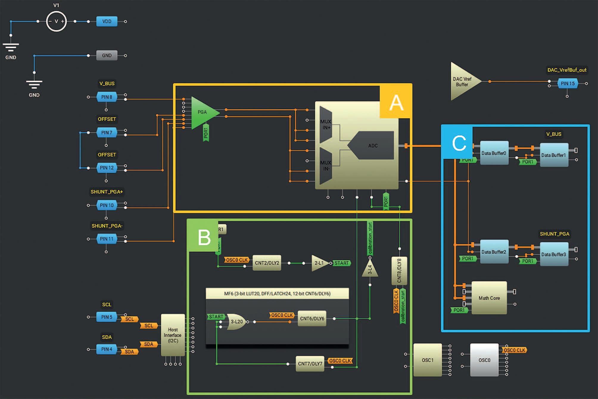
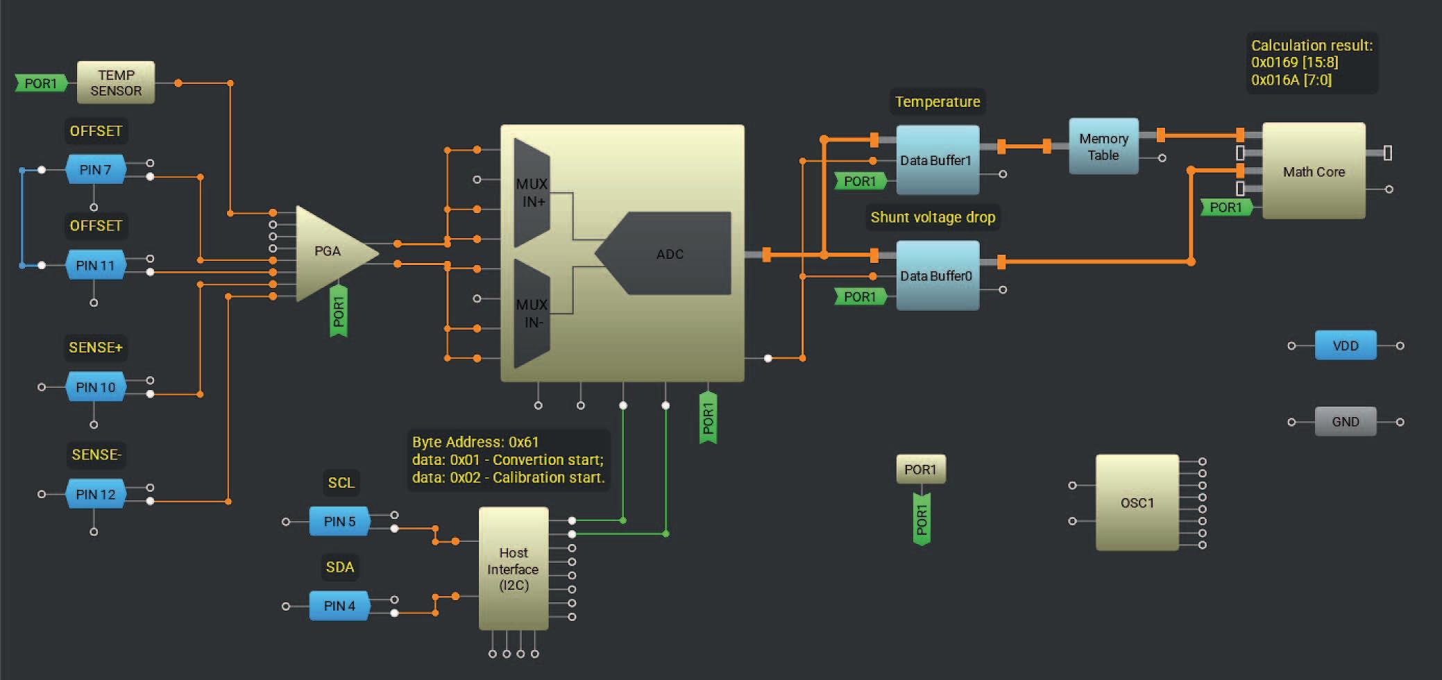
This design shown in Figure 1 is intended to interface with an MCU via I²C and can be divided conceptually into the following blocks:
Block A: Responsible for digitizing incoming analog signals. Notably, the Programmable Gain Amplifier (PGA) can be reconfigured through I²C, allowing individual gain adjustment for each measurement channel based on the specific characteristics of the signals being measured.
Block B: Manages the ADC control logic, ensuring proper initiation of the ADC. The SLG47011V also offers offset compensation capabilities for differential measurements. This block oversees timing and the correct operation of offset compensation during current measurement.
Block C: Handles the storage and the processing of digitized data. Buffers 0 to 3 store digitized data (from the ADC) and function as filters by updating data based on a moving average principle. The MathCore performs power calculations by multiplying the digital outputs of the voltage and current.


The results from each Buffer can be read via I²C and subsequently displayed through the MCU, or connected to a computer to establish a monitoring system. The solution shown in Figure 2 makes it possible to measure voltages up to 20V and currents up to 4A, provided that the PGA
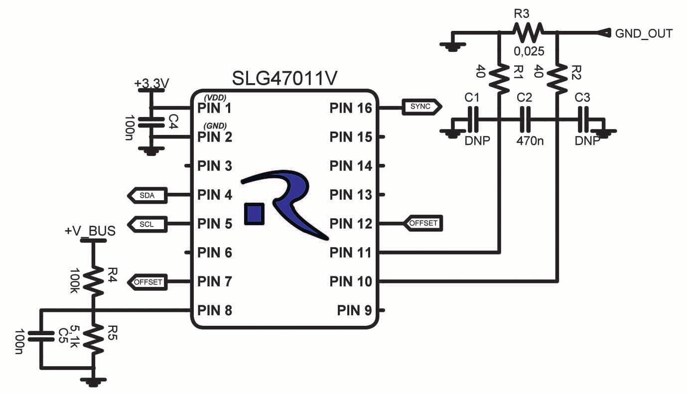
gain is switched via I²C depending on the current, namely: x32 for currents up to 1A, x8 for currents from 1A to 3A, and x4 for 4A. Otherwise, this circuit can measure currents up to 1A with a gain of x32. It is possible to reduce the gain to x16, thereby increasing the maximum measured current to 2A. However, since the initial design is based on overwriting the gain via I²C, it is important that the gain needs to be overwritten for both channel 3


(which is responsible for measuring the current) and channel 2, as it is responsible for calibrating the offset for channel 3. The input voltage is applied to the +V_BUS pin and is designed for a 4V to 20V voltage range.
Pins 7 and 8 must be connected together as they are responsible for the offset calibration.
Pin 16 (Sync) serves as a signal pin that controls when the MCU can access the SLG47011. Communication with the chip via I²C is only possible when Pin 16 is LOW. R3 is a shunt resistor from which the current is measured.
The MathCore read data is converted using the following formula: where:

M = data read from MathCore
Ge = gain of channel 3
It is also possible to read voltage and current values from Buffers 0 and 3, and they will be averaged in the same manner as the Buffer following the MathCore.
However, since two buffers are connected in series for the current, 16 bytes are averaged over 14 bits.
The read voltage is converted using the following formula: where:

ADCVbus = data read from Buffer 1
N = ADC resolution
The read current is converted using the following formula:

where:
ADCSHUNT = data read from Buffer 3
DEMO BOARD FUNCTIONAL DESCRIPTION
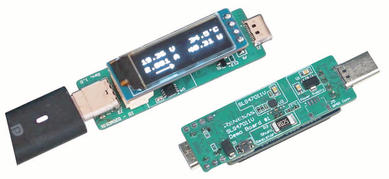
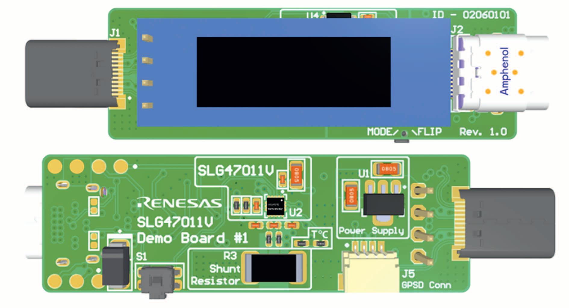
A practical demonstration of the SLG47011V's voltage, current, and power measurement capabilities can be seen in the SLG47011V Demo Board #1, which features an MCU to read and display data from the chip, along with the necessary components for accurate measurements. Three boards were tested for voltage and current measurement accuracy, and the results are described below.
Features
• Power delivery compatible (up to 28V, 5A)
• Voltage, current, power, and temperature measurements
• Measurements in both directions (plug and receptacle connection)
• 128 x 32 OLED monochrome display
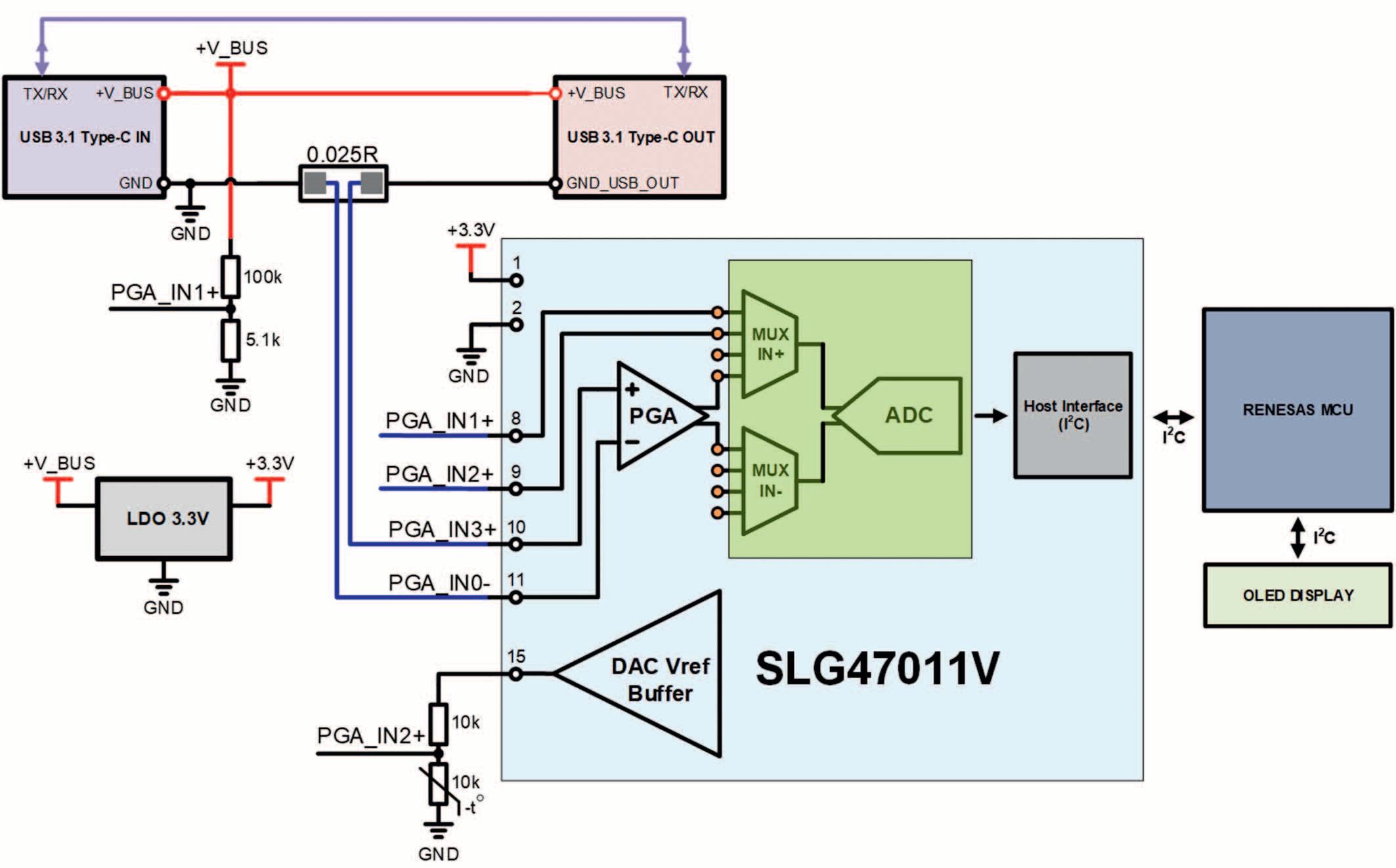
Table 2: Current Measurements Data
A simplified functional diagram is shown in Figure 4.
MEASUREMENT ACCURACY
Voltage and current measurements were performed on three different boards to gather statistics on accuracy (see Table 1 and Table 2).
CUSTOMIZATION FEATURES
As mentioned previously, the SLG47011V is a configurable logic IC, which allows for the implementation of advanced features such as watchdog functionality, overvoltage/overtemperature protection, among others, unlike other chips typically used in electrical parameter monitoring systems. This enhanced design is utilized for the application note (AN-CM-375 Voltage, Current, Power, and Temperature Monitor). This configuration not only allows for making simple measurements but also includes fault detection for the measured
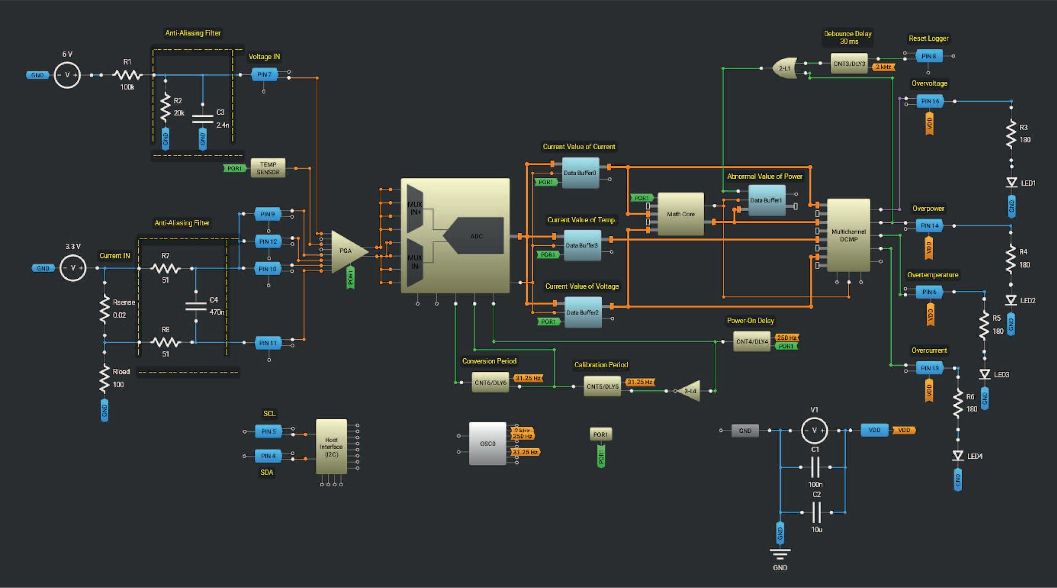
signals and outputs a fault signal externally as needed.
Another feature is the ability to measure the current on a copper pad (refer to ANCM-394 Current Sensing with Cu Trace).
In addition to the standard offset compensation available through the Memory Table and MathCore, it is also possible to measure current with the ability to compensate for temperature drift as well.
In conclusion, the SLG47011V offers a flexible and efficient solution for current, voltage, and power measurement applications. Its configurable logic, along with features like offset compensation, temperature drift correction, and fault detection, makes it a reliable choice for monitoring systems. The option to integrate additional functions, such as watchdog timers and
overvoltage/overtemperature protection, adds to its adaptability. With its programmability and high integration, the SLG47011V provides a practical platform for creating accurate, real-time monitoring solutions across various applications. ■ Renesas | www.renesas.com



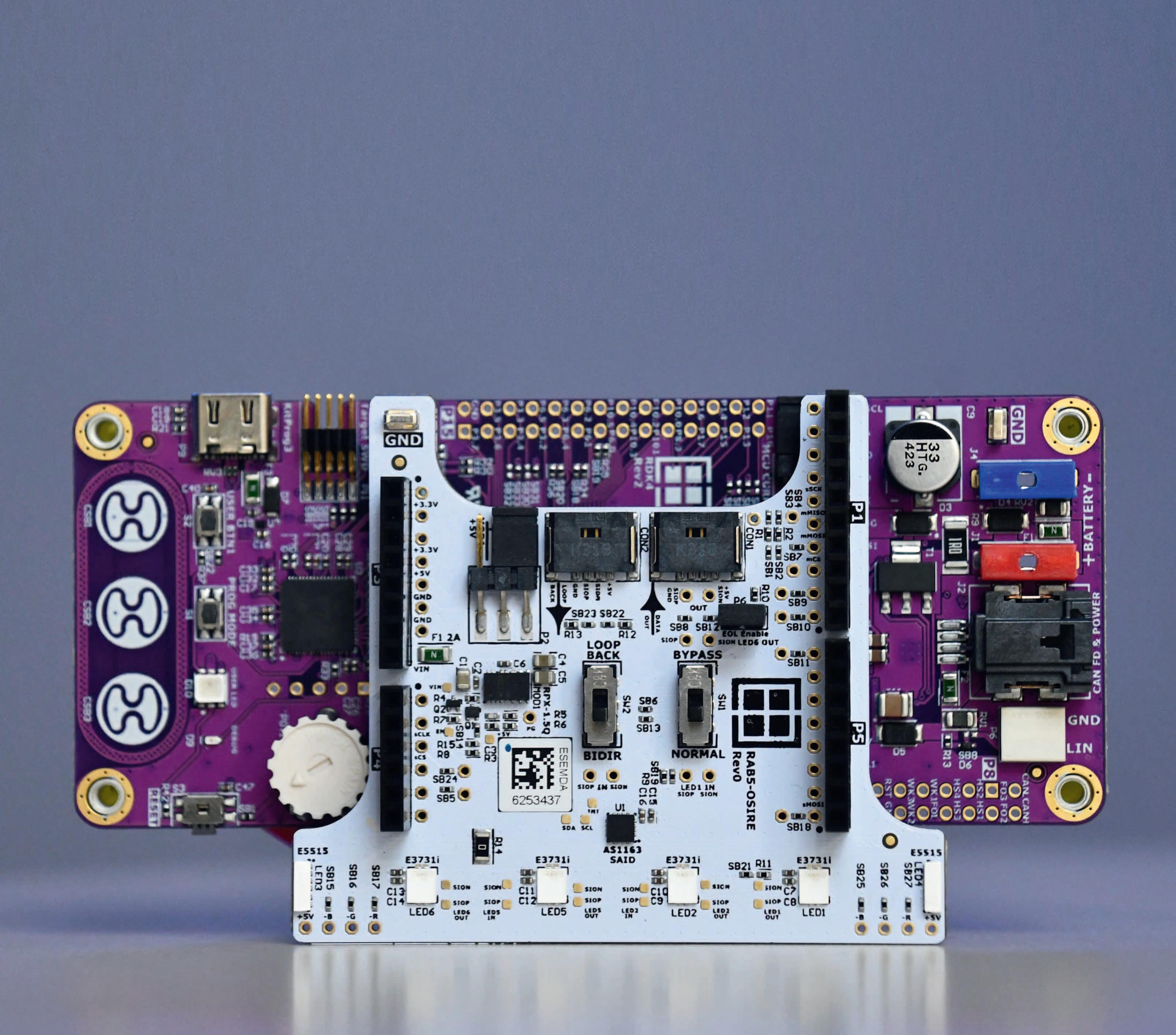
This article explores how the combination of ams OSRAM’s OSIRE® LED series and Rutronik’s modular development approach with the Adapter Board RAB5 OSIRE provide a robust platform for developers to implement scalable, intelligent lighting systems across automotive and industrial sectors.
Author: Stephan Menze, Head of Global Innovation Management, Rutronik
As embedded systems continue to evolve toward increased intelligence and connectivity, the role of LED technology has grown significantly. No longer just a source of light, LEDs are now integral components in human-machine interfaces, safety systems, and adaptive environments. From the automotive cabin to the smart factory floor, lighting is becoming programmable, responsive, and deeply embedded into system architectures.
The market for LEDs today spans a wide range of use cases. In the automotive sector, ambient interior lighting has become a defining element of the user experience. LEDs are used to create visually compelling environments that are both aesthetically pleasing and functionally adaptive. Lighting zones can dynamically respond to driving modes, user prefer-

ences, or environmental conditions, requiring a high degree of programmability and integration.
In industrial settings, LED systems contribute to operational efficiency by integrating into smart production environments. Adaptive illumination can respond to real-time sensor data, enhancing safety and reducing energy consumption. These applications are aligned with the principles of Industry 4.0 or the upcoming 5.0,
where LEDs must operate reliably under varying conditions and interface seamlessly with IIoT infrastructures.
Integrating LEDs into these systems involves challenges such as maintaining consistent performance, achieving precise color calibration, and scaling across complex installations. The OSIRE® series from ams OSRAM addresses these challenges with a combination of precision, intelligence, and robustness.
Developed for both automotive and industrial environments, the OSIRE® LED series allows each unit to be individually addressable, enabling precise control over color, brightness, and dynamic lighting effects. This capability supports advanced lighting scenarios driven by user interac tion or environmental feedback.
Each LED integrates a temperature sensor that ensures color stability by actively compensating for thermal shifts across RGB channels. This is particularly crucial in automotive interiors or industrial equip ment where fluctuating conditions could otherwise compromise output quality.
Designed with scalability in mind, up to 1,000 OSIRE® LEDs can operate on a sin gle communication bus. Combined with AEC-Q qualification, the series is tailored for mission-critical and large-scale appli cations that demand reliability and con figurability.
When combined with Rutronik’s RDK4 base board, which features the Infineon PSOC™ 4100S Max automotive microcontroller, the RAB5 becomes a powerful prototyping solution. This setup delivers robust communication, low power consumption, and a cost-efficient Arm® Cortex® M0+ core for real-time control and data processing.
The platform is particularly suited for HMI elements, motor control systems with integrated lighting, and intelligent signaling. Developers benefit from a streamlined development flow, real-world simulation capabilities, and a path to faster validation – all critical in reducing time to market and ensuring compliance.
The RAB5 OSIRE development environment is designed to meet the evolving needs of electronics engineers by offering both technical sophistication and practical usability.
Comprehensive documentation, an intuitive GUI, and flexible hardware interfaces allow for agile development, system customization, and rapid prototyping.
By addressing integration complexity and supporting modular expansion, the platform fosters innovation without compromising the quality, compliance, or performance required in professional embedded systems.
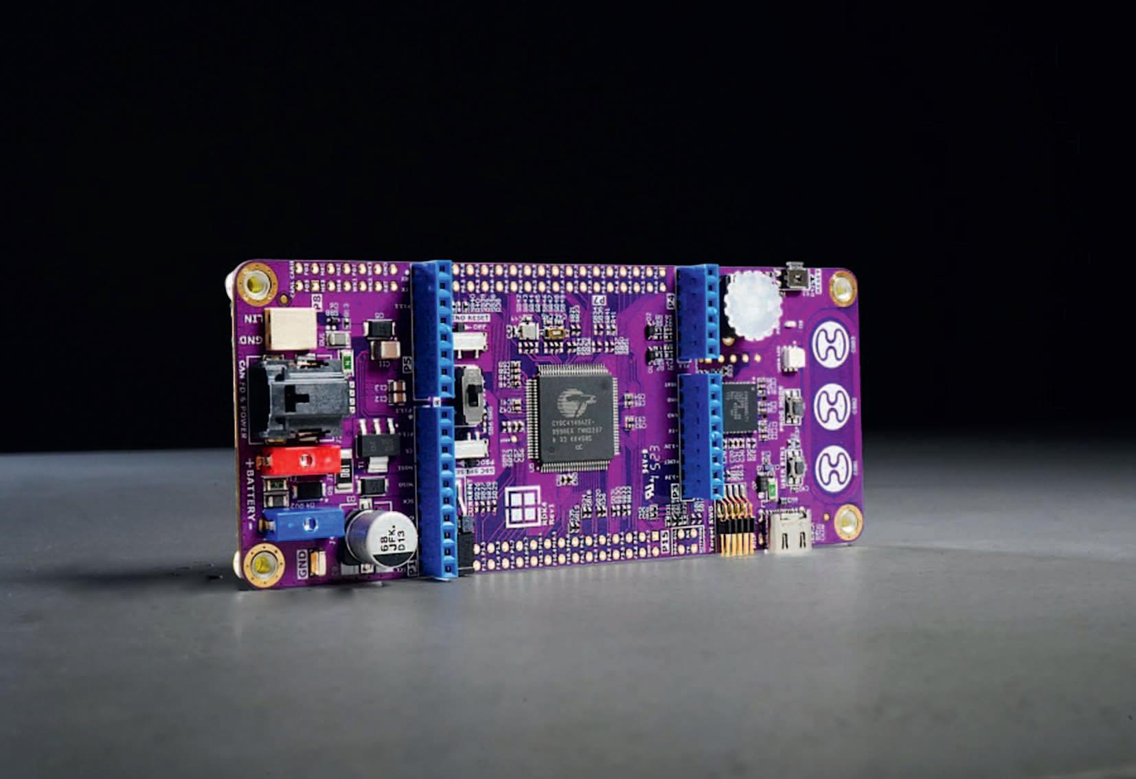
Rutronik’s RAB5 Adapter Board serves as a modular evaluation interface, streamlining prototyping and integration of OSIRE® LEDs. Its compatibility with Arduino connectors enables straightforward integration with various base and adapter boards, such as the RDK4 platform. This modularity supports scalable development and testing across a wide spectrum of applications.
RAB5 includes on-board features like temperature compensation, diagnostics, and auto-addressing. An open communication protocol ensures that developers are not locked into proprietary ecosystems, and the accompanying GUI from ams OSRAM simplifies programming and real-time control of each LED.


While originally designed for automotive lighting, the OSIRE® and RAB5 platform is also ideal for smart home devices, rail systems, and industrial HMI applications. Its programmability and modularity enable developers to build responsive RGB-enabled interfaces and lighting that reflects operational states or user commands. Because all components, including drivers, converters, and connectors, are part of Rutronik’s unified portfolio, developers benefit from simplified sourcing and ensured compatibility throughout the system design process.


As industries continue to embrace automation, personalization, and connected infrastructure, advanced LED systems will play a central role. The combination of ams OSRAM’s OSIRE® series and Rutronik’s development ecosystem provides a reliable, scalable foundation for implementing intelligent lighting across sectors. Focused on programmability, system compatibility, and performance, these tools are already shaping the next generation of embedded lighting technologies. The global LED market continues to expand, driven by innovations in embedded electronics and the need for smarter, energy-efficient lighting.
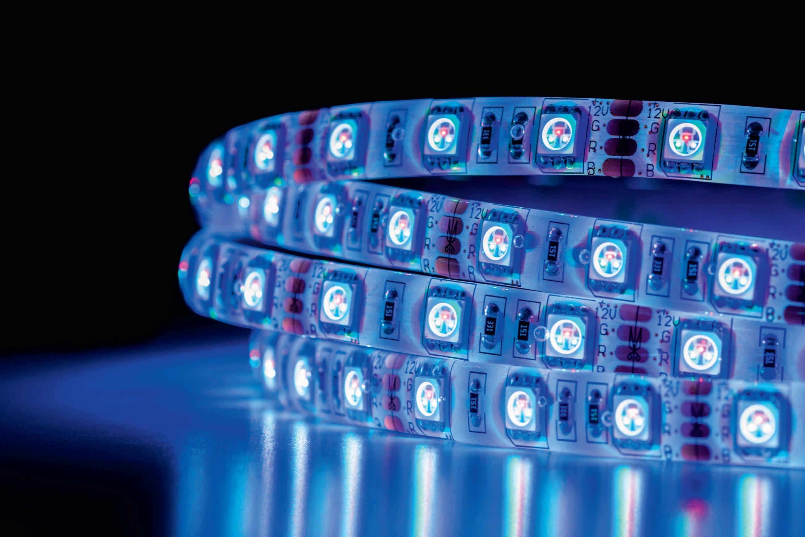
In the automotive sector, LEDs are no longer just a design element – they enhance the driving experience, provide visual cues for safety, and support new user interfaces. Whether illuminating door panels, dashboards, or touch-sensitive controls, LEDs help reinforce brand identity and increase user engagement. Meanwhile, industrial applications for LEDs are equally transformative. In automated production lines and smart factories, intelligent lighting systems adapt to machine states, operator presence, and environmental conditions in real time. This dynamic response not only improves productivity but also reduces energy usage, contributing to more sustainable manufacturing environments. High-performance, programmable LEDs like the OSIRE® series are central to building these adaptive lighting frameworks.
The OSIRE® LEDs are engineered to meet these complex requirements. Their smart features extend beyond basic illumination: integrated algorithms manage brightness and color shifts, ensuring visual consistency across all devices in a chain. Developers can configure color transitions, pulse patterns, and synchronization behaviors across multiple units using the graphical interface or direct software integration.
This opens the door to highly customized lighting profiles for different use cases, from mood lighting in vehicles to status indicators in industrial settings. The ability to connect up to 1,000 LEDs on a single bus is particularly valuable in large installations where wiring complexity and latency must be minimized. This is achieved through an efficient, open communication protocol that supports auto-addressing and real-time diagnostics. Because of these features, the OSIRE® platform scales gracefully from simple prototypes to fully integrated commercial systems.
The design philosophy behind Rutronik System Solutions emphasizes modularity and ease of use. The Adapter Board RAB5, built around OSIRE® LEDs, exemplifies this approach. When paired with the RDK4 Base Board, developers gain access to a full-featured microcontroller environment powered by Infineon’s PSOC™ 4100S Max. This MCU balances cost and performance and is ideal for applications that require real-time control, signal processing, and system diagnostics.
This development ecosystem is tailored to support a wide variety of projects – ranging from ambient lighting in electric vehicles to control panels in industrial machinery.
The Arduino-compatible interface ensures that developers can rapidly integrate additional modules or sensors as needed. Whether it’s for experimenting with RGB light behaviors, evaluating temperature responses, or simulating real-world deployment conditions, the platform is ready to support sophisticated engineering workflows. As demand grows for user-centric design in both automotive and industrial domains, LEDs are increasingly being recognized as a strategic design element rather than just a utility. Developers are tasked with delivering solutions that not only meet technical standards but also contribute to intuitive, aesthetically pleasing, and adaptive user experiences.
In this context, the Adapter Board RAB5 offers a compelling path forward. It merges precision hardware, intelligent control, and a developer-friendly ecosystem to accelerate time-to-market without compromising performance. For engineers building the next generation of lighting systems – whether for passenger cabins, production halls, or smart appliances – this toolkit delivers both the flexibility and reliability required in today’s competitive development environment.
■ Rutronik www.rutronik.com

Electric motors are widely utilized across various applications that are integral to our contemporary way of life and have a substantial influence on it. Almost half of the electricity worldwide is consumed by applications that include electric motors and motor control systems. Considering this, electric motor manufacturers are now mandated to adhere to policies concerning energy consumption and efficiency. Additionally, they are encouraged to utilize environmentally friendly materials and adopt sustainable manufacturing processes. This shift in focus is propelling the development of more energy-efficient electric motors, electronics and algorithms that allow motors to function at superior efficiency levels while retaining a compact design. These trends are indicative of the continuous progress in motor technology, with the aim of enhancing efficiency, performance and sustainability across a broad spectrum of applications.
Author: Pramit Nandy, Product Marketing Manager, Microchip Technology
The shift towards electric vehicles and the demand for energy-efficient systems are driving the adoption of electric motors across various industries. The motors are no longer limited to traditional applications. Below are some modernday motor applications.
The integration of motor systems with Internet of Things (IoT) and Artificial Intelligence (AI) technologies is paving the way for predictive maintenance, real-time surveillance and the enhancement of motor performance.
The growing emphasis on energy efficiency has spurred the creation of high-efficiency motors, featuring innovative designs and superior materials, which contribute to a reduction in energy usage and carbon emissions.
Compact and lightweight motors are becoming increasingly significant, especially in sectors like automotive, aerospace and industrial, as well as certain consumer applications where space and weight conservation are crucial. Progress in motor control algorithms, such as model-based predictive control and advanced sensorless control, are boosting motor performance, accuracy and agility.
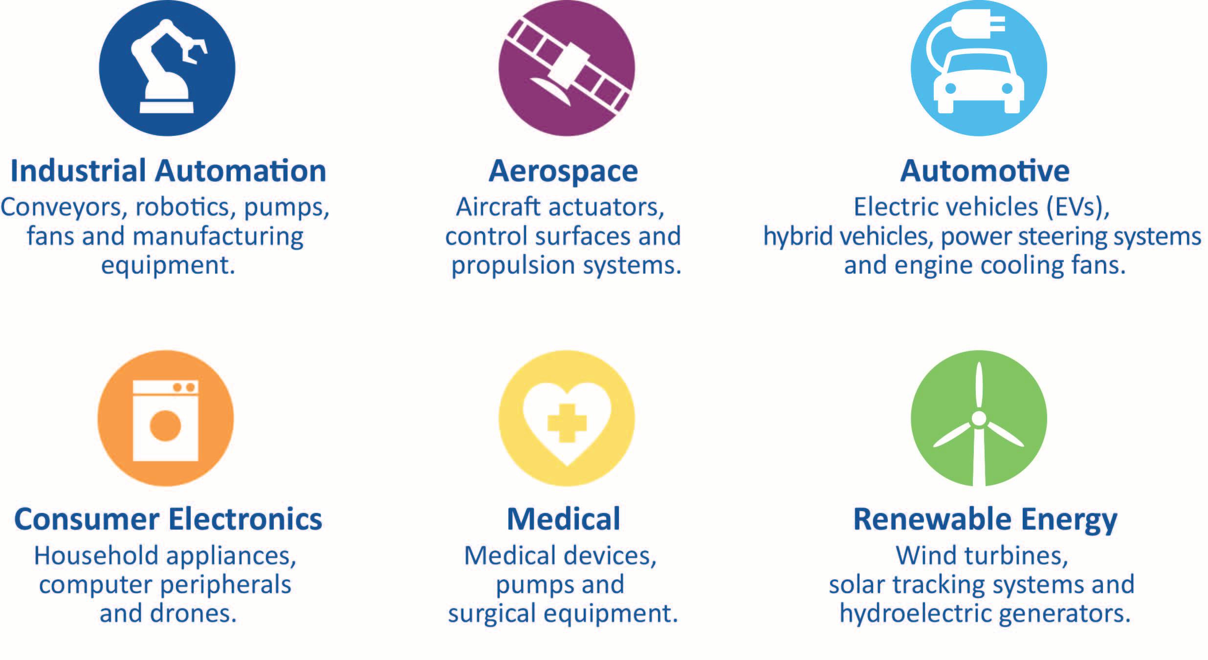

The latest trends in motor control applications are driving advancements in technology, which includes the use of integrated motor drivers. Integrated motor drivers combine all the control and analog interface functions required for implementing complex motor control algorithms and typically include an advanced microcontroller (MCU) capable of running sensorless Field Oriented Control (FOC), a 3-phase gate driver and, sometimes, a transceiver for communication.
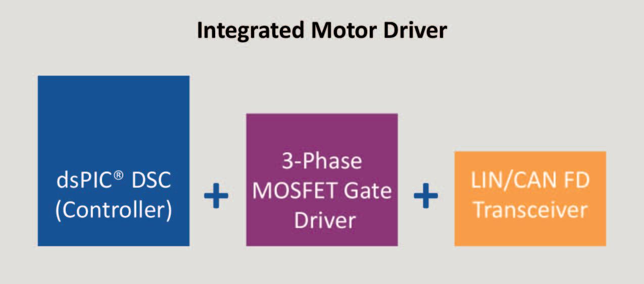
Integrated motor drivers serve a crucial role in various applications and industries. Overall, the demand for integrated motor drivers is driven by their ability to streamline design, reduce costs, enhance performance, conserve space, improve reliability and facilitate seamless integration with other systems.
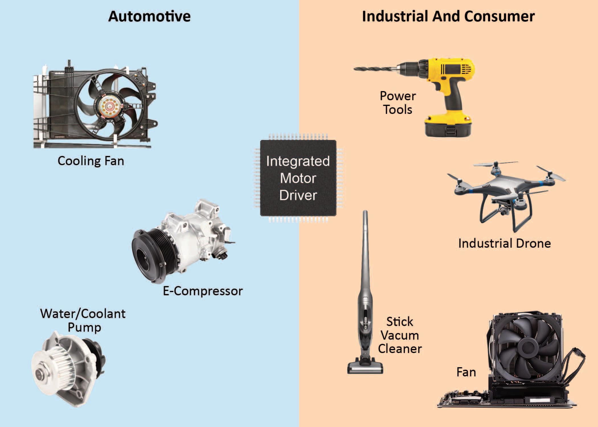
They offer an all-encompassing solution for efficient, compact and reliable motor control applications across various industries. Integrated motor drivers play an important role in improving performance, efficiency and safety in automotive, industrial and electric vehicle (EV) applications. In the automotive sector, they enhance Electric Power Steering (EPS), braking, HVAC and engine cooling systems. In industrial environments, they facilitate precise control in robotics, battery operated pumps, compressors and machine tools. In EVs (Electric vehicles), these microcontrollers optimize motor control,
battery management, regenerative braking, thermal management, power efficiency and system integration and include diagnostic and safety features. Here are some key reasons integrated motor drivers are necessary components for a variety of applications: The compact size, cost-effectiveness, advanced control algorithms and built-in safety features of integrated motor control microcontrollers make them essential in these sectors, driving advancements and contributing to improved performance, energy efficiency, reliability and overall system integration.
Microchip Technology has unveiled a new series of integrated motor drivers, powered by the dsPIC® Digital Signal Controller (DSC). These devices are designed to streamline the implementation of efficient, real-time embedded motor control systems in applications where space is at a premium. The motor drivers, which incorporate a dsPIC33 DSC, a full-bridge MOSFET gate driver and an optional LIN or CAN FD transceiver, simplify the design process by reducing the number of components, PCB (Printed Circuit Board) size and overall system complexity.
These integrated motor driver devices can operate on a single power supply of up to 29V (operation) and 40V (transient) and deliver high CPU (Central Processing Unit) performance, operating between 70 and 100 MHz. They are designed to facilitate the efficient implementation of Field Oriented Control (FOC) and other advanced motor control algorithms. The inbuilt 3.3V Low Dropout (LDO) voltage regulator powers the dsPIC DSC, eliminating the need for an external LDO.
To accelerate the design process, Microchip offers a comprehensive ecosystem of motor control software and hardware development tools.
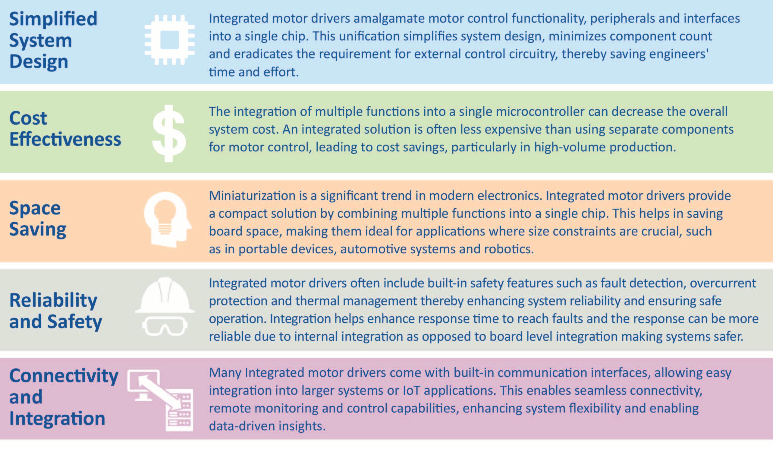


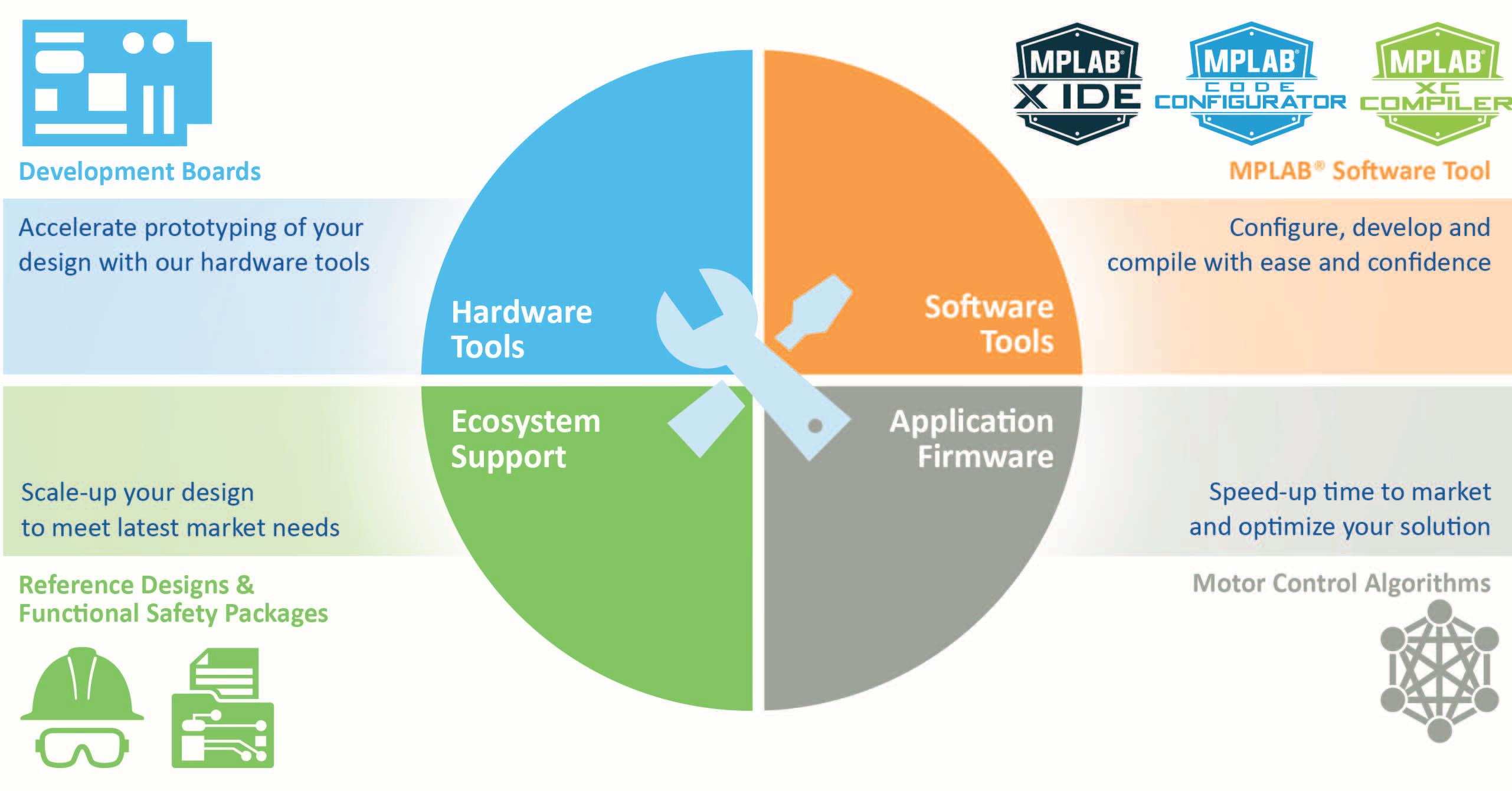
The dsPIC33CK Motor Control Starter Kit (MCSK) and the MCLV-48V-300W Development Board are two new dsPIC33-based integrated motor driver development boards that offer flexible control options and facilitate rapid prototyping of motor control applications.
The MPLAB® motorBench® Development Suite, a complimentary GUI-based software development tool for FOC, measures critical motor parameters, automatically tunes feedback control gains and generates source code. The latest version, v2.45, introduces a new feature, Zero-Speed/ Maximum Torque (ZS/MT), which maximizes torque output from the motor, eliminating the need for Hall or magnetic sensors.
Microchip also offers complimentary MPLAB® Device Blocks for MATLAB® Simulink® that can be used to generate optimized code from models for dsPIC DSCs and other Microchip MCUs. The expanding portfolio of dsPIC DSC based motor control reference designs now includes several motor control applications offering ready-to-use solutions to help accelerate development time. Below is an example showing an automotive cooling fan reference design which uses the dsPIC33CDVL64MC106 Integrated Motor Driver with LIN Transceiver. For further details about Microchip’s integrated motor drivers, please visit the dsPIC® DSC-Based integrated motor drivers webpage.
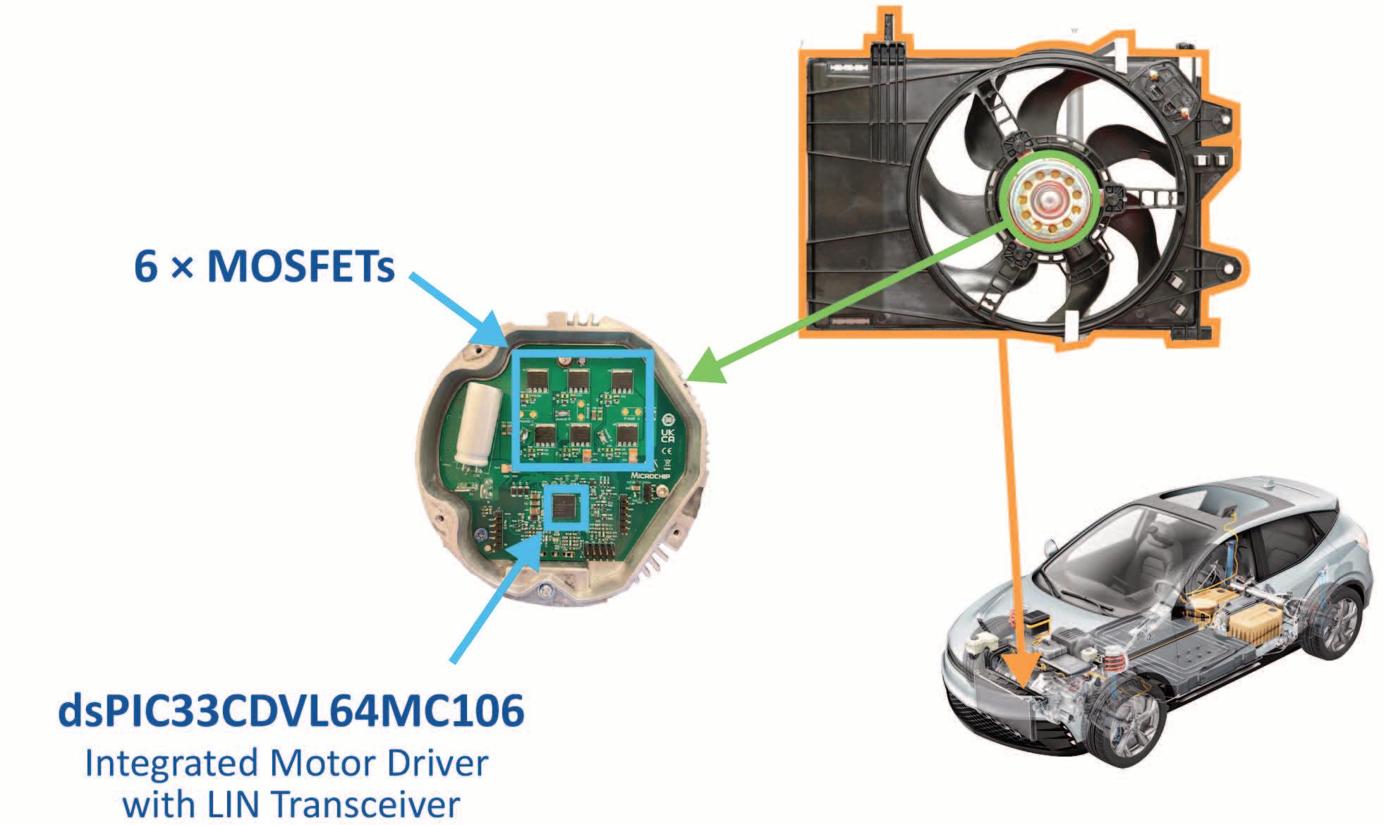
The future of motor control is poised for exciting advancements as technology continues to evolve. Motor control applications are becoming increasingly efficient, intelligent, precise and interconnected. Ongoing research and development, along with improvements in semiconductor technology, control algorithms and system integration are set to further enhance the complexity of motor control applications in both hardware and software aspects. To address escalating hardware complexity, there is a growing demand for integrated motor drivers that include a controller, 3-phase MOSFET gate driver and some form of connectivity. This integration will facilitate the delivery of high-power and precision, making it apt for a broad spectrum of applications ranging from industrial machinery to electric vehicles. With the inclusion of communication interfaces, these integrated motor drivers can be seamlessly designed into a networked environment, enabling remote control and monitoring. Microchip Technology's integrated motor drivers present a holistic solution for motor control applications, offering superior performance, adaptability, and connectivity. These drivers stand as a testament to Microchip's dedication to delivering innovative and effective solutions in response to the constantly evolving technological landscape.
■ Microchip Technology www.microchip.com


Many challenges in electronics production and applications can be solved with the comprehensive Flex Suppressor product family: Signal integrity can be easily enhanced, crosstalk minimized, and the reliability of electronic devices increased.
Author: Daniele Carnevale, Corporate Product Sales Manager Inductors, Rutronik
Every electronics developer is familiar with the issue of interference from frequencies on cables or printed circuit boards. Fortunately, there is now a flexible and easy-to-use solution to this problem: the Flex Suppressor series. Regardless of whether it is to pass EMC tests or to improve the overall application performance through protected signal integrity or improved communication range.
Flex Suppressor comes in a range of shapes and variants, e.g. in various sheet sizes and as meter-long rolls and strips. In the following, the application is presented on the basis of three application areas.
One of the biggest challenges in electronics is electromagnetic interference (EMI). This type of interference can significantly impact the performance of electronic devices, thereby leading to malfunctions.
When an application is impacted by electromagnetic interference, applying a piece of Flex Suppressor to the source or path of the interference can immediately and effectively resolve the issue. Due to its special structure and material composition, Flex Suppressor absorbs unwanted radiation emissions in a range from 30 MHz to 1 GHz.
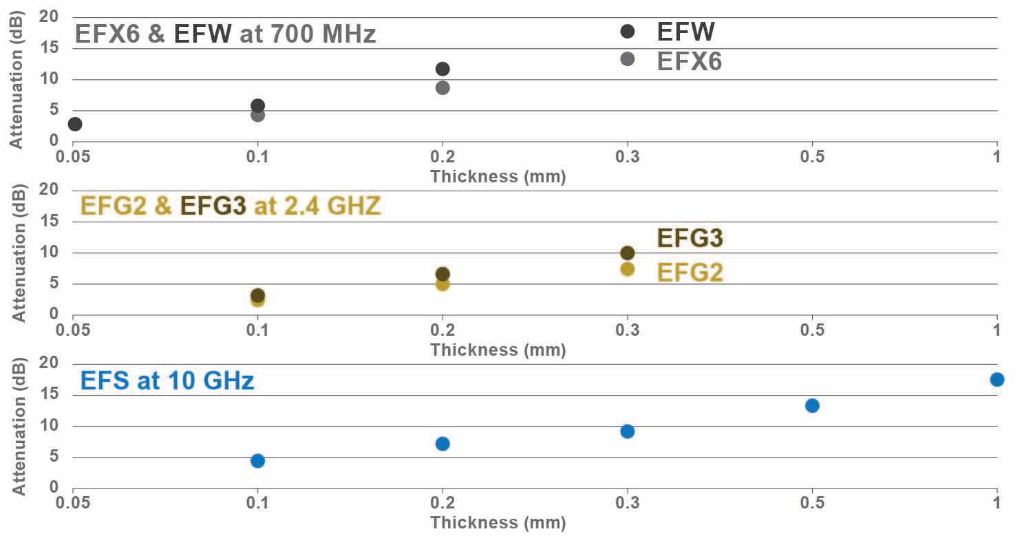

This results in more stable and reliable operation, particularly in applications subjected to high levels of electromagnetic stress.
The most important factors to consider in this application are the frequency range being covered and the space available for the thickness of Flex Suppressor.
A thicker piece of Flex Suppressor is more efficient, but also more expensive. To find the optimum cost/performance ratio, the thickness must be weighed against the attenuation in the desired frequency range (Figure 1).
An application scenario is shown in Figure 2. In this case, the integrated circuit (IC) is the noise source.
Due to reflections from the metal package, the EMI emission in the FM band exceeds the EMI regulations. An effective countermeasure is to attach a piece of Flex Suppressor (e.g. EFF4(039)) directly above the source of interference.
As the demand for better reception sensitivity in high-capacity and fast mobile devices grows, noise-canceling measures in high-frequency bands are becoming increasingly crucial.
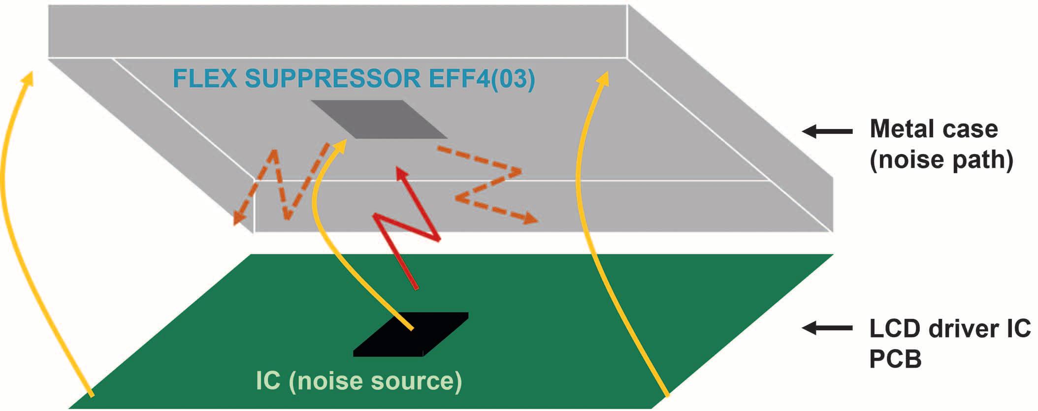
:
• Protects against the effects of radiated noise at the source or on the transmission line
• Is effective against high-frequency interference generated by electronic devices, and
• Minimizes crosstalk.
This improves signal purity and increases the reliability of data transmission. And this is vital for applications in high-frequency technology, telecommunications, and other fields where precise signal transmission is essential. The range of possible applications is almost unlimited. The thin, flexible material can be cut into any shape and is ideal for use in portable devices or in areas with limited space. Further, Flex Suppressor can be used in a wide frequency range from MHz to GHz. Figure 3 shows the effect of Flex Suppressor on the RFID antenna of a cell phone.
In this test, the cell phone is used as the transmitter and the antenna (read/write device) as the receiver. The actual communication range can be determined by moving the cell phone toward the antenna. Flex Suppressor helps to triple the communication range. This can determine whether direct contact is still necessary for NFC or RFID, or if gesture-based interactions can be conducted from a distance.
Electronic devices and systems are often impacted by interference from unshielded cables. This interference can be caused by electromagnetic fields emitted by neighboring cables or external sources. The latest addition to the Flex Suppressor family is the flexible EST tape, a suppressor tape. A major advantage is its ease of use: The EST tape is simply wrapped around the outer surface of a cable and can be
shortened to the required length without the need for cutting tools. It is therefore ideal for quickly and easily checking EMI noise sources and for EMI troubleshooting, especially during the test phase.
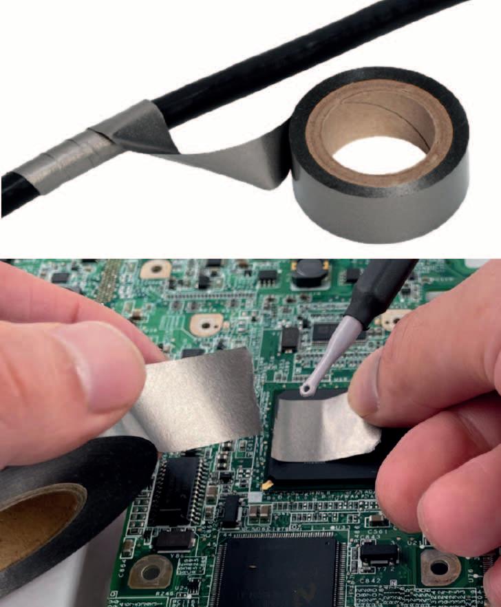
EST tape is easy to use and mainly applied for troubleshooting in the test phase.
Developers can use it to carry out initial tests in order to determine how much shielding is required for the respective application.
In summary, using Flex Suppressor products helps manage and optimize the electromagnetic environment of electronic systems, ensuring reliable and trouble-free performance
■ Rutronik www.rutronik.com

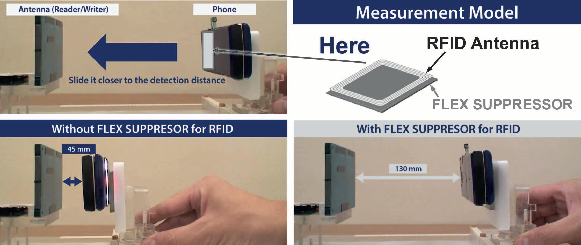


The rising popularity of time of flight (TOF) cameras in industrial applications, particularly in robotics, is attributed to their exceptional depth computing and infrared (IR) imaging capabilities. Despite these advantages, the inherent complexity of the optical system often constrains the field of view, limiting standalone functionality. This article discusses a 3D image stitching algorithm designed for a supporting host processor, eliminating the need for cloud computation.
This algorithm seamlessly combines IR and depth data from multiple TOF cameras in real time, producing a continuous, high quality 3D image with an expanded field of view beyond standalone units.
The stitched 3D data enables the application of state-of-the-art deep-learning networks – particularly valuable in mobile robotics applications – to revolutionize the visualization and interaction with the 3D environment.
Authors:
Rajesh Mahapatra, Senior Manager
Anil Sripadarao, Principal Engineer
Swastik Mahapatra, Senior Engineer
Analog Devices
Time of flight (TOF) cameras stand out as exceptional range imaging systems, utilizing TOF techniques to determine the distance between a camera and each point in an image. This is achieved by measuring the round-trip time of an artificial light signal emitted by a laser or an LED. TOF cameras offer precise depth information, making them valuable tools for applications where accurate distance measurement and 3D visualization are crucial, such as robotics and industrial technology applications, including collision detection and human detection over 270° field of view (FOV) for safety.
The ADTF3175 TOF sensor can achieve a calibrated 75° FOV. However, challenges arise when an application’s FOV exceeds this region, requiring multiple sensors.
Integrating data from individual sensors to provide comprehensive analytics for the entire view can pose difficulties. One potential solution involves having sensors execute an algorithm on a partial FOV and transmitting the output to a host for collation. Yet this approach faces issues such as overlap zones, dead zones, and communication latencies, making it a complex problem to address effectively.
An alternate approach involves stitching the captured data from all sensors into a single image and subsequently applying detection algorithms on the stitched image. This process can be offloaded to a separate host processor, relieving the sensor units from the computational load and providing room for advanced analytics and other processing options. However, it’s important to note that traditional

image stitching algorithms are inherently complex and can consume a significant portion of the host processor’s computational power. Furthermore, sending to and stitching in the cloud is not possible in many applications due to privacy reasons. Analog Devices’ algorithmic solution can stitch the depth and IR images from the different sensors, using the point cloud projections of the depth data. This involves transforming the captured data using camera extrinsic positions and projecting it back into 2D space, resulting in a single continuous image.
This approach results in minimal computation, which helps achieve real-time operating speeds on the edge and ensures that the compute capacity of the host processor remains available for other advanced analytics.
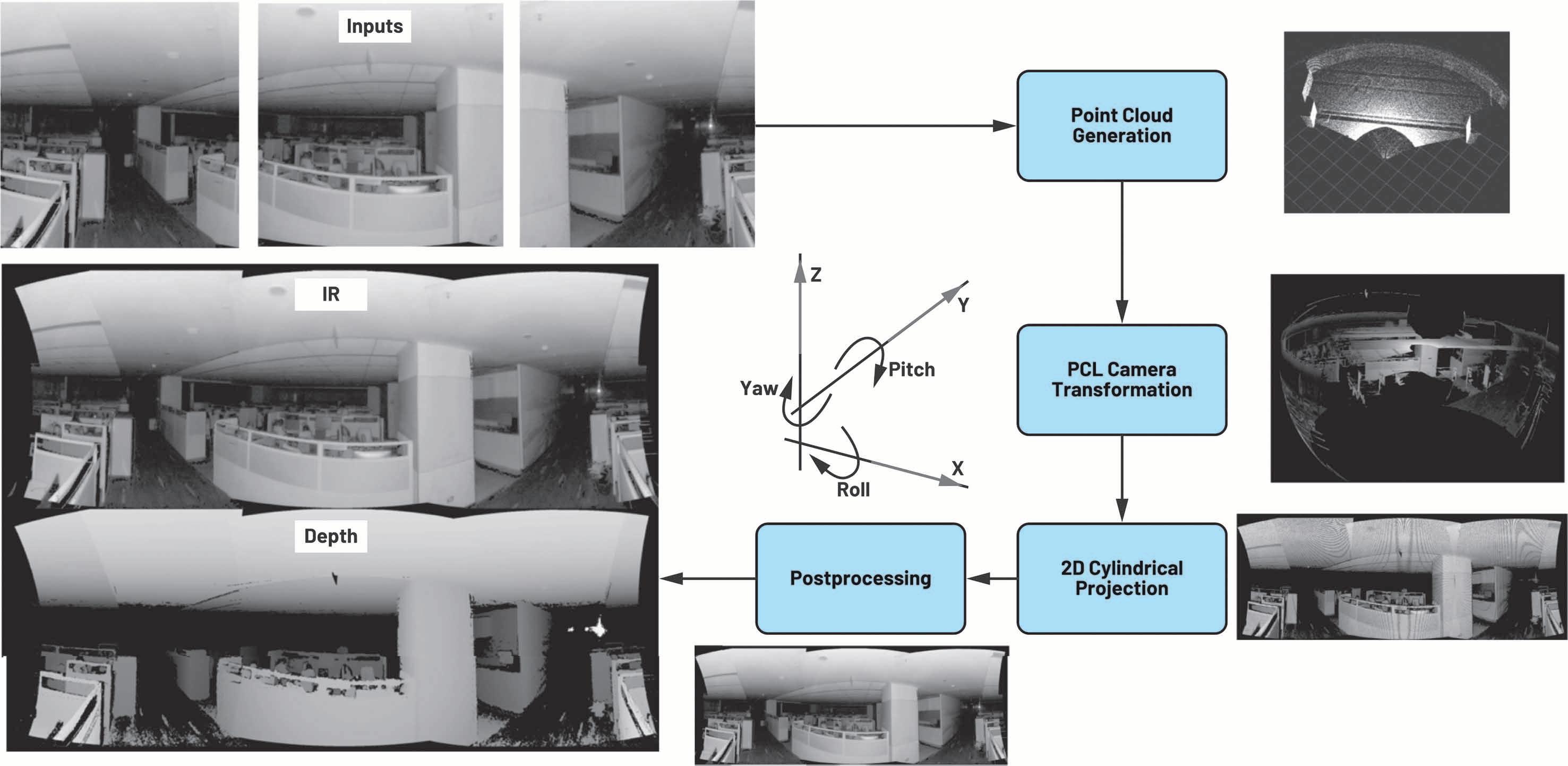
A DESCRIPTION OF A SOLUTION ADI’s 3D TOF solution operates in four stages (see Figure 1):
1. Preprocess IR and depth data: Time synchronization and preprocessing of IR and depth data.
2 Project depth data into 3D point cloud: Utilize camera intrinsic parameters to project depth data into a 3D point cloud.
3. Transform and merge points: Transform points using the camera’s extrinsic positions and merge overlapping regions.
4. Project point cloud into 2D image: Employ cylindrical projection to project the point cloud back into a 2D image.
SYSTEM AND ALGORITHM CHALLENGES AND SOLUTIONS
Host Receives Depth and IR Frames
A host machine is connected to multiple TOF sensors over a high speed connection such as USB. It collects depth and IR frames and stores them in a queue.
Synchronize Depth and IR Data
Depth and IR frames from each sensor received by the host are captured at different instances of time. To avoid temporal mismatch due to the movement of objects, inputs from all sensors need to be synchronized to the same instance of time. A time synchronizer module is used that matches incoming frames based on timestamps from the queue.


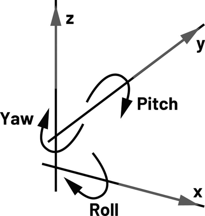
Project-to-Point Cloud
The point cloud is generated on the host using the synchronized depth data for each sensor. Each point cloud is then transformed (translated and rotated) based on its respective camera positions (see Figure 2) in the real world. Then these transformed point clouds are merged to form one single continuous point cloud covering the combined FOV of sensors (see Figure 3).
3D to 2D Projection
The combined point cloud of the FOV is projected to a 2D canvas using a cylindrical projection algorithm also known as front view projection (see Figure 4).


In other words, the algorithm projects each point of the merged point cloud onto a pixel in the 2D plane, which results in a single continuous panoramic image covering the combined field of view of all the sensors.
The depth data of the ADTF3175 has an invalid depth value of 0 mm for points that are beyond the operational range of the sensor (8000 mm).

A depth value of 8000 mm (the largest depth supported by the camera) was assigned to all the invalid points on the depth image and a point cloud was generated with it.

This results in two 2D stitched images: one for stitched IR and another for stitched depth images projected onto 2D planes.
Projecting the 3D combined point cloud onto a 2D image still does not give good quality images. The images have distortions and noise. This affects visual quality and would also adversely affect any algorithm that runs on the projection. The three key issues (see Figure 5) and the fixes are documented in the following sections.
This results in large void regions on the depth image and forms incomplete point clouds.
This ensured that there were no gaps in the point cloud.
While projecting the 3D point cloud onto a 2D plane, there are unmapped/unfilled regions in the 2D image. Many point cloud (3D) pixels get mapped to the same 2D pixel and hence several 2D pixels remain blank. This results in the stretch pattern shown in Figure 6. To fix this, a 3 × 3 filter was used that fills the unmapped pixels with the average IR/depth value of its neighboring 8 pixels that have valid values. This resulted in a more complete output image formation and artifacts were removed (see Figure 6).
Because of the cylindrical projection algorithm, many points on the overlapping region end up getting the same resting coordinates on the 2D projected output. This creates noise as the background pixels overlap the foreground ones. To fix this, the radial distance of each point is compared with the existing point, and the point is replaced only if the distance from the camera origin is smaller than the existing point.
Ted to retain only the foreground points and improve the projection quality (see Figure 7).
This algorithm can stitch images from different cameras with less than 5° of overlap compared to a minimum of 20° of overlap as needed by traditional key
points matching algorithms. This approach needs very little computation, making it an ideal candidate for edge systems. The integrity of the depth data is retained post-stitching as there is no image distortion. This solution further supports the modular implementation of the ADTF3175 sensors to obtain the desired FOV with minimal loss.


The FOV expansion is not confined to the horizontal dimension, and the same technique can be used to expand the view vertically to obtain true spherical vision. The solution runs on an Arm® V8, 6-core edge CPU at 10 fps for four sensors providing 275° FOV. The frame rate goes up to 30 fps when only two sensors are used. One of the key benefits of this approach is the massive computation gain achieved –more than 3× gain in basic computation (see Table 1).
Figure 8 and Figure 9 show some results obtained using this solution.
Analog Devices

About the authors:
Rajesh Mahapatra has 30+ years of work experience and is working in the Software and Security Group of Analog Devices, Bangalore. He is passionate about solving customer problems using algorithms and embedded software working on ADI hardware solutions. He works closely with NGOs to plant trees and to provide training to urban economically challenged people to generate livelihood. He has five patents in the system, image processing, and computer vision area. Anil Sripadarao joined Analog Devices in 2007 and is working for the Software and Security Group of ADI, Bangalore. His areas of interest include audio/video codecs, AI/ML, computer vision algorithms, and robotics. He holds six patents in image processing and computer vision domain.
Swastik Mahapatra is a senior machine learning engineer with the Software and Security Group. He joined Analog Devices in 2018 and has worked on various computer-vision technologies and robotic safety solutions. He has worked extensively on deep-learning edgeinference framework development, robotic applications development, and is proficient in convolutional neural networks. His professional interests include algorithm development for computer vision, 3D vision, machine learning, and robotics.
Engage with like-minded members and ADI technology experts in our online community, EngineerZone®. Expand your network, ask your tough design questions, share your expertise, browse our rich knowledge base, or read about new technologies and the engineers behind them in one of our blogs.
Visit https://ez.analog.com
Table 1: Computational Complexity Comparison: Traditional Algorithms vs. Proposed Algorithm for a 512 × 512 QMP Input
References
“Analog Devices 3DToF ADTF31xx.” GitHub, Inc.
“Analog Devices 3DToF Floor Detector.” GitHub, Inc.
“Analog Devices 3DToF Image Stitching.” GitHub, Inc.
“Analog Devices 3DToF Safety Bubble Detector.” GitHub, Inc.
“Analog Devices 3D ToF Software Suite.” GitHub, Inc.
He, Yingshen, Ge Li, Yiting Shao, Jing Wang, Yueru Chen, and


Shan Liu. “A Point Cloud Compression Framework via Spherical Projection.” 2020 IEEE International Conference on Visual Communications and Image Processing, 2020.
Industrial Vision Technology. Analog Devices, Inc. Topiwala, Anirudh. “Spherical Projection for Point Clouds.” Towards Data Science, March 2020.
For over four decades I have witnessed transformative shifts in the power electronics landscape. Beginning with bipolar transistors, moving through MOSFETs and into the realm of wide band gap (WBG) semiconductors such as silicon carbide (SiC) and gallium nitride (GaN). Each technological evolution has unlocked higher performance, greater efficiency, and the miniaturization of power systems. But today, we stand at the threshold of what could be the next quantum leap in power device performance towards the mythical 99.99% efficiency: the use of synthetic diamond as a semiconductor material, a really exciting new concept for power electronics engineers.
Author: Patrick Le Fèvre
IS THE USE OF DIAMONDS IN SEMICONDUCTORS REALISTIC?
The idea might sound exotic – if not farfetched – but after all, diamonds are traditionally associated with jewelry, industrial applications such as abrasives, and machinery for cutting, drilling, grinding, and polishing or in laboratories for highpressure experiments though not with power conversion systems or radio-frequency amplifiers.
However, for many years, the scientific community has acknowledged diamonds as the premier material for heat dissipation, exhibiting thermal conductivity that significantly surpasses conventional materials such as silicon. Nevertheless, the
material's inherent hardness and the complexity of its processing had previously rendered it unsuitable for utilization in the field of semiconductor technology. Before delving into the subsequent discussion on performance and benefits, it is imperative to provide a synopsis of the evolution of diamond utilization in technological applications. The narrative commences in 1954 when General Electric (GE) successfully created the first synthetic diamond using the High Pressure High Temperature (HPHT) method, marking the inaugural instance of human fabrication of diamonds. Subsequent to this landmark, the 1980s bore witness to the inaugural expansion of diamonds by the Chemical Vapor Deposition (CVD) method, which
was subsequently followed by the exploration of doping processes in the 1990s. After this, those involved in the development of synthetic diamonds have expanded their knowledge of this material in terms of characterization, manufacturing, and processing.
Yet, advances in materials science and fabrication techniques are rapidly transforming synthetic diamond into a contender for the future of semiconductors. Let’s explore why diamond is considered a material of superlatives, how it compares with conventional and established WBG semiconductors (SiC and GaN), and what hurdles remain before it can reach commercial maturity.
We used to say that the evolution of power electronics is like a staircase with major leapfrogs bringing in new technology from research to market to improve performance, and diamond semiconductors might be considered as the next step, however some consider it far too big a challenge to become reality.
It’s important to note that SiC and GaN weren’t overnight successes either.
I remember when SiC power diodes first entered the market in the late 1990s, they were expensive, difficult to manufacture, and had reliability issues. GaN’s commercial journey began later, finding initial adoption in RF applications and later evolving into high-efficiency power transistors for everything from fast chargers to datacenter power supplies.
There’s no doubt that conventional silicon semiconductor technology is well established and is permanently improving with new technologies, though the success of SiC and GaN that was driven by an industry that required higher voltages, higher efficiency and higher switching frequencies to reduce the size of the final equipment. Today SiC and GaN are in everything from EVs to solar inverters. WBG materials offered significant size, weight, and power (SWaP) benefits, and we all enjoy powerful, energy efficient, and compact USB adapters.
GaN brought advantages in high frequency switching due to its high electron mobility and low capacitance. Meanwhile, SiC found its place in medium to high voltage ranges, replacing IGBTs and silicon MOSFETs in applications like electric vehicles and industrial drives. However, both SiC and GaN have their limits and some applications operating in high temperatures and harsh environments may require higher performance levels and robustness, and this is where diamond’s properties appear not just superior – but transformative.
To understand diamond's potential, we must start with material science. In semiconductor technology, the performance of material for high-power, high-frequency, or high-temperature applications is governed by key physical properties.
Presenting the fundamental properties of Silicon, Silicon Carbide, Gallium Nitride and Diamond, in the table (Figure 1) we selected four key parameters, making it easy to compare the performance and benefits of the different materials:
The band gap, which is indicative of a material's capacity to conduct electricity, serves as a critical criterion in determining its suitability for environments characterized by high temperatures or high energies.
It also opens the door for devices rated for 10kV, 20kV or even 50kV use, potentially revolutionizing high-voltage DC (HVDC) transmission, electric railways, and grid-tied energy systems.
Electron mobility is defined as the speed of electron movement under an electric field. It is a critical component of electronic switching and signal propagation, which occurs rapidly.
The enhancement of electron mobility in
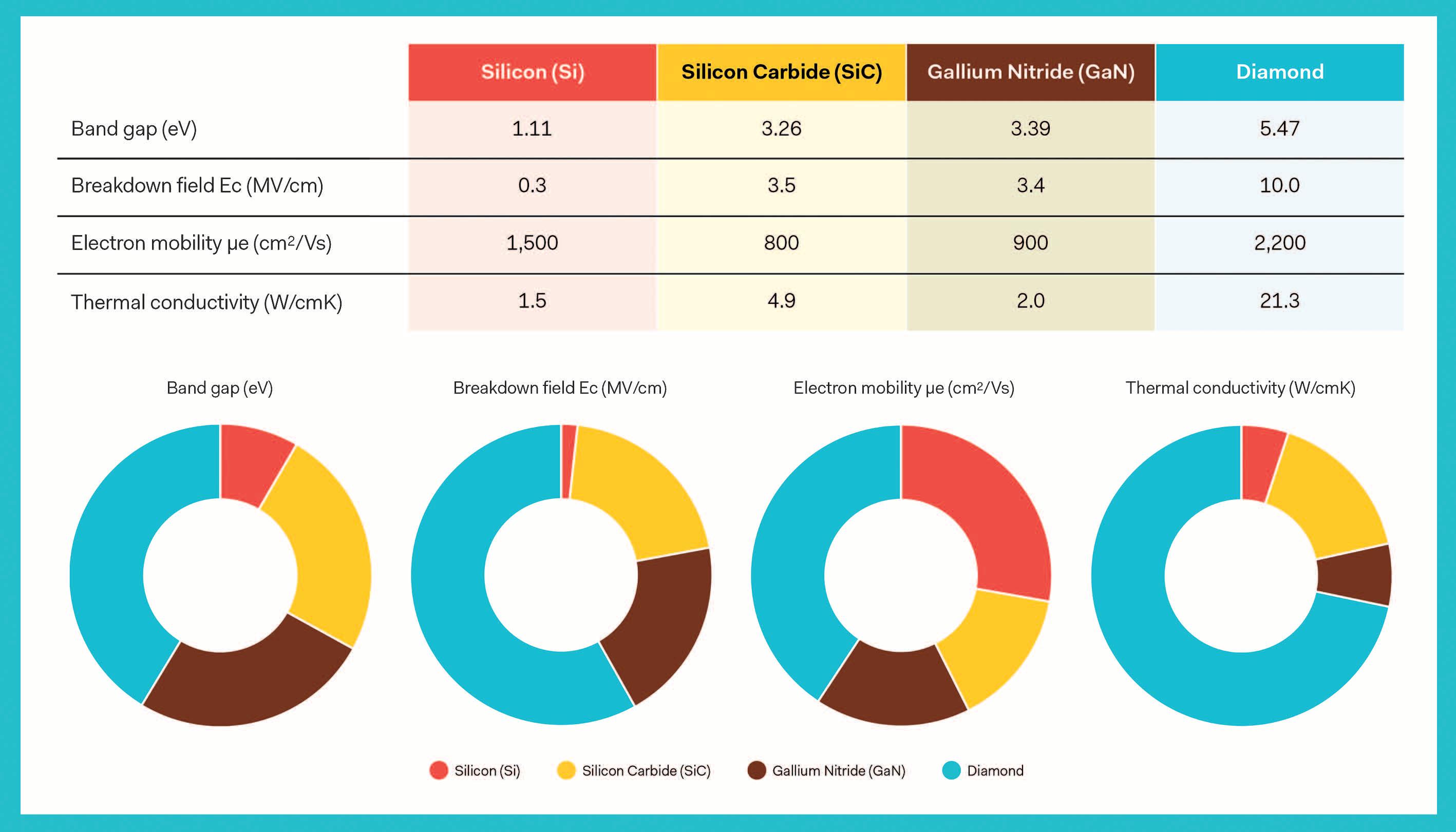
A wider band gap is indicative of superior resistance to current leakage and breakdown, which is critical for applications in extreme conditions. Here, diamond outshines every other material by far. Its wide bandgap of 5.5 eV allows devices to operate at higher voltages and temperatures.
The Breakdown field is a measurement of a material's resilience against electrical stress prior to the occurrence of conductivity. It is imperative to note that higher breakdown field values are of essence for devices operating at elevated voltages, particularly in the domain of power electronics. This is due to the fact that ensuring optimal performance under extreme electrical loads is of the utmost importance.
The theoretical critical electric field of diamond is nearly 10 MV/cm which is three times higher than that of GaN or SiC and over 30 times that of silicon. This allows devices to be thinner for the same voltage rating, reducing resistance and improving efficiency.


these devices leads to an improvement in the performance of digital circuits and high-frequency analog devices. Although GaN and diamond have similar electron mobilities, diamond devices may benefit from higher saturated velocities, enabling extremely fast switching with low on-resistance and reduced losses. This could push switching frequencies to new heights, further miniaturizing magnetic components like transformers and inductors.
Thermal conductivity is a material property that quantifies its capacity for heat transfer. In the field of electronics, high thermal conductivity is of essence. This property is crucial for the effective dissipation of heat, thereby preventing overheating and enhancing the reliability and longevity of devices.
Diamond’s thermal conductivity of 20 W/cmK is the highest known of any material, making it exceptionally good at heat dissipation, a constant challenge in power electronics.
As we all know, thermal management is one of the most expensive and limiting factors in high-performance systems.
GaN, for instance, often requires exotic substrates like silicon carbide to avoid overheating. Diamond’s unparalleled ability to dissipate heat could lead to devices operating at temperatures exceeding 400°C without degradation, enabling more compact and rugged systems, especially in aerospace and high temperatures applications.
Despite the hype, diamond semiconductors are not yet in mainstream production. But significant progress has been made in the past decade, particularly in synthetic diamond fabrication, led by chemical vapor deposition (CVD). CVD enables the production of large-area, ultra-pure single-crystal diamond wafers – a major prerequisite for reliable semiconductor devices.
Today, diamond Schottky diodes and power FETs transistors have been demonstrated in labs with promising characteristics. However full commercialization is still in early stages, limited by fabrication cost, defect density, doping control, and scalability. However, the latest research is very promising.
In hindsight, I feel the same way as I did when SiC and GaN were in the research stages. As a power electronics engineer, I dove into numerous papers on wideband gap technology and its promises, I wrote articles and presented them at conferences to share my enthusiasm within the power electronics community. Twenty years later, these promises have become a commercial reality.
After years of fundamental research, the utilization of diamonds in the semiconductor industry is now moving to the next step, which involves pre-industrialization and the development of an ecosystem to support future commercial products.
It is challenging if not impossible to list all the major steps recently occurring within the diamond semiconductor industry. As a French national working for a European company owned by the Japanese company COSEL, I would like to share some notable projects in Japan and France (EU) but for sure many similar steps have taken place in USA.
It is known that the first power circuit containing synthetic diamond semiconductors has been developed by a research team from a Japanese university. Following an exploration of the hypothesis that diamond semiconductors have
the potential to outperform silicon and other materials currently in use, led by Professor Makoto Kasu, a team at Saga University who initiated an investigation into diamond semiconductors and developed a functional n-channel MOSFET transistor made with a diamond.
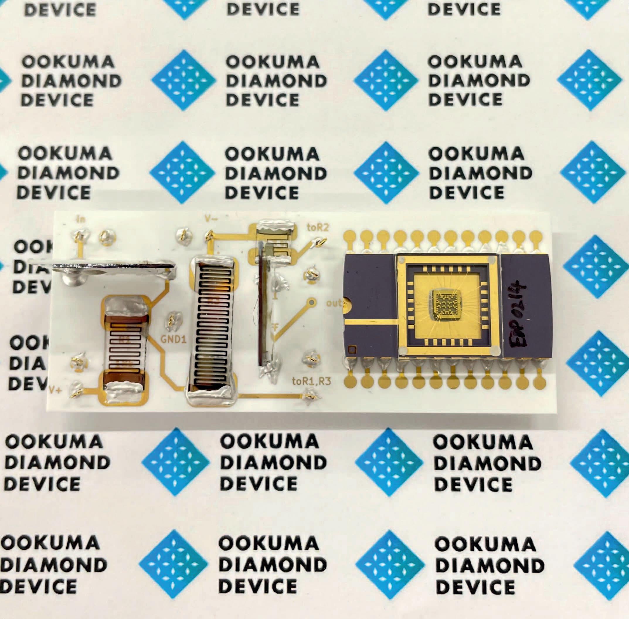

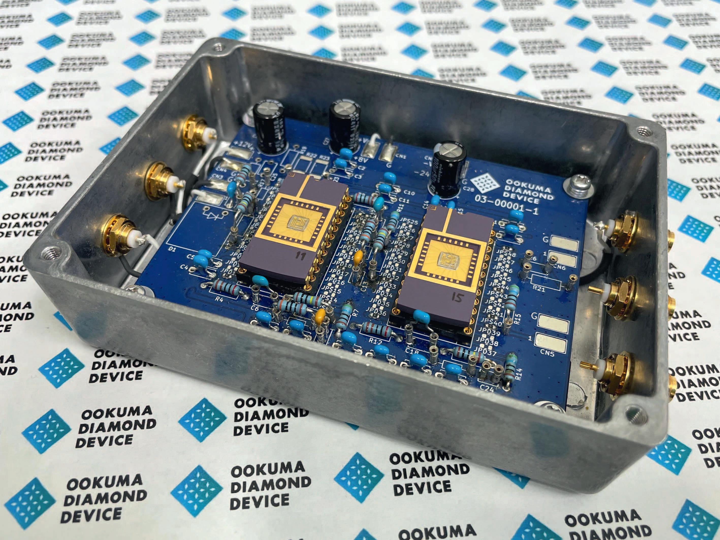

Another seminal moment in the Japanese semiconductor industry's evolution was the cessation of operations at the Fukushima Daiichi Nuclear Power Station (NPS), precipitated by the tsunami that followed the Great East Japan Earthquake on March 11, 2011. In the context of the decommissioning process for the reactors, a research initiative was initiated in 2012 with the objective of developing diamond semiconductors that could function in the harsh environment of the damaged NPS, which was contaminated with high radiation.
The initiative was made possible by the convergence of technical expertise from prominent organizations such as the AIST, the Japan Atomic Energy Agency (JAEA), Hokkaido University, and the High Energy Accelerator Research Organization (KEK).
The objective was unambiguous: to engineer a critical approach, monitoring systems utilizing diamond semiconductors capable of withstanding high radiation levels, thereby providing detailed data, including neutron dose on fuel debris. This endeavor was undertaken to ensure the planning for debris removal was both safer and more efficient.
As part of this project, Ookuma Diamond Device Co., Ltd., a startup founded jointly by Hokkaido University and the National Institute of Advanced Industrial Science and Technology (AIST) established a vertically integrated system for manufacturing diamond semiconductors, covering everything from substrate design to assembly of the world's first differential amplifier circuit using diamond semiconductors, which has been confirmed to operate for a long-term period under a high temperature environment (300°C) resulting in the latest prototype shown in Figures 2 and 3.
In early 2025, reports emerged of a significant development in the field of advanced semiconductor technology. The National Institute of Advanced Industrial Science and Technology (AIST), in collaboration with Honda R&D, successfully fabricated a prototype of a H-terminated diamond MOSFET. This breakthrough marked the first demonstration of ampere-level highspeed switching operation, a major advancement in the realm of semiconductor research and development. The Keita Takaesu et al. research team increased the size of the substrate and developed parallel wiring technology to increase the current (doi: 10.35848/1882-0786/adba3a).
In the future, they plan to apply this technology to the next generation of mobile power devices. They are currently in the process of verifying and validating the preliminary results, which will pave the way for higher-current diamond MOSFETs.
In Europe several projects took place but it’s wise to mention the framework program for research and innovation called Horizon 2020 which took place in January 2014. The objectives of Horizon 2020 were to strengthen the EU's scientific and technological foundations, to create a European Research Area with free circulation of researchers and knowledge and drive the EU towards a knowledge society and competitive economy.
As part of Horizon 2020, a sub project Green Electronics with Diamond Power Devices, coordinated by the French Centre National de la Recherche Scientifique (CNRS) aimed to explore the possibilities and feasibility of the promising technology and so formed a consortium. The consortium gathers experts on power device design, diamond growth and characterization, packaging and testing as well as an innovative end-user.


Most of the partners were also involved in SiC or GaN technology, allowing the project to benefit from their ample experience and achievements in wide bandgap semiconductors.
Among the notable reports published under this project, and as part of the next phase, I would like to mention the French company Diamfab, founded in March 2019 by CEO Gauthier Chicot and CTO Khaled Driche, housed at the Institute Néel-CNRS. Since its inception, Diamfab has established a collaborative network contributing to the technological development of synthesizing diamonds and developing cutting-edge components like Schottky diodes and MOSFET transistors (Figure 4).
In terms of research, it’s worth mentioning
the collaboration between the Institute Néel (CNRS), the Plasma and Energy Conversion Laboratory (LAPLACE, CNRS/ Toulouse INP/University) and DIAMFAB who have designed a diamond transistor achieving a record volume current conduction of 50 mA. The component is a junction field-effect transistor (JFET) using volume conduction. The team succeeded in obtaining homogeneous layers of diamond doped with boron, without any harmful defects. They were thus able to increase the useful volume of the transistor and its gate, which reaches 14.7 mm with 24 parallel fingers. The transistor is no longer a simple miniature demonstrator, but a real usable component, which prevails a good future for diamond transistor technology (Figure 5).
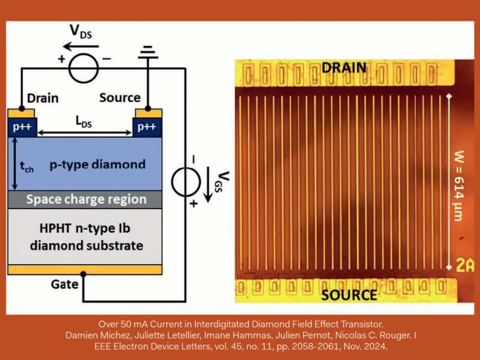
(Left) Cross-sectional schematic of an elementary diamond JFET with the electrical measurement setup. (Right) Optical microscopy top view of interdigitated diamond JFET at the end of the fabrication process.
References:
Powerbox (PRBX): https://www.prbx.com
SAGA University: https://www.saga-u.ac.jp/en
Ookuma Diamond Device Co., Ltd.: https://ookuma-dd.com/en
Honda R&D: https://global.honda/en/RandD
VISION: WHERE COULD DIAMOND LEAD US?
Imagine EV inverters with 99.9% efficiency, switching at 1 MHz, requiring no bulky cooling systems. Picture ultra-compact space power modules surviving extreme temperatures and radiation on the Moon or Mars. Or envisage smart grids operating at 100 kV with embedded sensors powered by diamond ICs. Such visions may sound futuristic – but so did SiC/GaN 25 years ago.
If development continues, diamondbased semiconductors could become the platform of choice for ultra-high-power, high-reliability applications within the next two decades. Governments and private sector players are increasingly investing in diamond R&D, viewing it as a strategic technology with both energy and defense implications.
NOT JUST A SPARKLE, BUT A BEACON In the world of semiconductors, the material defines the limits - and diamond redefines those limits. While commercial readiness may be years away, the performance ceiling that diamond promises is too significant to ignore. As power electronics continues to demand higher efficiency, higher voltage, and smaller form factors, the industry must keep an open eye on this gem of a material. Just as we transitioned from silicon to Wide Band Gap SiC and GaN to enable breakthroughs in electric mobility and renewables, the next frontier may well be forged in carbon’s hardest form – paving the way to the ultimate power semiconductor platform.
And just like we did with previous waves of innovation, those of us in the field must prepare – not just with technical readiness, but with imagination and curiosity.
■
National Institute of Advanced Industrial Science and Technology (AIST): https://www.aist.go.jp/index_en.html
Ampere-class double pulse testing of half-inch H-terminated diamond MOSFET chip
Applied Physics Express 18, 036502 (2025): https://doi.org/10.35848/1882-0786/adba3a CNRS - Institut Néel: https://neel.cnrs.fr/en/institut-neel Laboratoire Plasma et Conversion d’Energie: https://www.laplace.univ-tlse.fr/en/home DIAMFAB: https://diamfab.com
Over 50 mA current in interdigitated diamond field effect transistor
Damien Michez et al. – IEEE Electron Device Letters, 2024, 45 (11), pp.2058-2061. ⟨10.1109/LED.2024.3453504⟩.: https://hal.science/hal-04687646v1
