The
J.E. Smyth
https://ebookmass.com/product/the-law-and-business-administration-incanada-15c-edition-j-e-smyth/
ebookmass.com
Contents
Preface
Acknowledgments
About the Authors
Chapter 1 Engineering the Power Delivery Network
1.1 What Is the Power Delivery Network (PDN) and Why Should I Care?
1.2 Engineering the PDN
1.3 “Working” or “Robust” PDN Design
1.4 Sculpting the PDN Impedance Profile
1.5 The Bottom Line Reference
Chapter 2 Essential Principles of Impedance for PDN Design
2.1 Why Do We Care About Impedance?
2.2 Impedance in the Frequency Domain
2.3 Calculating or Simulating Impedance
2.4 Real Circuit Components vs. Ideal Circuit Elements
2.5 The Series RLC Circuit
2.6 The Parallel RLC Circuit
2.7 The Resonant Properties of a Series and Parallel RLC Circuit
2.8 Examples of RLC Circuits and Real Capacitors
2.9 The PDN as Viewed by the Chip or by the Board
2.10 Transient Response
2.11 Advanced Topic: The Impedance Matrix
2.12 The Bottom Line
References
Chapter 3 Measuring Low Impedance
3.1 Why Do We Care About Measuring Low Impedance?
3.2 Measurements Based on the V/I Definition of Impedance
3.3 Measuring Impedance Based on the Reflection of Signals
3.4 Measuring Impedance with a VNA
3.5 Example: Measuring the Impedance of Two Leads in a DIP
3.6 Example: Measuring the Impedance of a Small Wire Loop
3 7 Limitations of VNA Impedance Measurements at Low Frequency
3.8 The Four-Point Kelvin Resistance Measurement Technique
3.9 The Two-Port Low Impedance Measurement Technique
3 10 Example: Measuring the Impedance of a 1-inch Diameter Copper Loop
3.11 Accounting for Fixture Artifacts
3.12 Example: Measured Inductance of a Via
3.13 Example: Small MLCC Capacitor on a Board
3.14 Advanced Topic: Measuring On-Die Capacitance
3.15 The Bottom Line
References
Chapter 4 Inductance and PDN Design
4.1 Why Do We Care About Inductance in PDN Design?
4.2 A Brief Review of Capacitance to Put Inductance in Perspective
4.3 What Is Inductance? Essential Principles of Magnetic Fields and Inductance
4.4 Impedance of an Inductor
4.5 The Quasi-Static Approximation for Inductance
4 6 Magnetic Field Density, B
4.7 Inductance and Energy in the Magnetic Field
4.8 Maxwell’s Equations and Loop Inductance
4.9 Internal and External Inductance and Skin Depth
4.10 Loop and Partial, Self- and Mutual Inductance
4.11 Uniform Round Conductors
4.12 Approximations for the Loop Inductance of Round Loops
4.13 Loop Inductance of Wide Conductors Close Together
4.14 Approximations for the Loop Inductance of Any Uniform Transmission Line
4.15 A Simple Rule of Thumb for Loop Inductance
4.16 Advanced Topic: Extracting Loop Inductance from the S-parameters Calculated with a 3D Field Solver
4.17 The Bottom Line References
Chapter 5 Practical Multi-Layer Ceramic Chip Capacitor Integration
5.1 Why Use Capacitors?
5.2 Equivalent Circuit Models for Real Capacitors
5 3 Combining Multiple Identical Capacitors in Parallel
5.4 The Parallel Resonance Frequency Between Two Different Capacitors
5.5 The Peak Impedance at the PRF
5.6 Engineering the Capacitance of a Capacitor
5.7 Capacitor Temperature and Voltage Stability
5.8 How Much Capacitance Is Enough?
5.9 The ESR of Real Capacitors: First- and Second-Order Models
5.10 Estimating the ESR of Capacitors from Spec Sheets
5 11 Controlled ESR Capacitors
5.12 Mounting Inductance of a Capacitor
5.13 Using Vendor-Supplied S-parameter Capacitor Models
5.14 How to Analyze Vendor-Supplied SParameter Models
5.15 Advanced Topics: A Higher Bandwidth Capacitor Model
5.16 The Bottom Line References
Chapter 6 Properties of Planes and Capacitors
6.1 The Key Role of Planes
6.2 Low-Frequency Property of Planes: Parallel Plate Capacitance
6.3 Low-Frequency Property of Planes: Fringe Field Capacitance
6.4 Low-Frequency Property of Planes: Fringe Field Capacitance in Power Puddles
6.5 Loop Inductance of Long, Narrow Cavities
6.6 Spreading Inductance in Wide Cavities
6.7 Extracting Spreading Inductance from a 3D Field Solver
6.8 Lumped-Circuit Series and Parallel SelfResonant Frequency
6 9 Exploring the Features of the Series LC Resonance
6.10 Spreading Inductance and Source Contact Location
6.11 Spreading Inductance Between Two Contact Points
6.12 The Interactions of a Capacitor and Cavities
6.13 The Role of Spreading Inductance: When Does Capacitor Location Matter?
6.14 Saturating the Spreading Inductance
6.15 Cavity Modal Resonances and Transmission Line Properties
6.16 Input Impedance of a Transmission Line and Modal Resonances
6.17 Modal Resonances and Attenuation
6.18 Cavity Modes in Two Dimensions
6.19 Advanced Topic: Using Transfer Impedance to Probe Spreading Inductance
6.20 The Bottom Line References
Chapter 7 Taming Signal Integrity Problems When Signals Change Return Planes
7.1 Signal Integrity and Planes
7.2 Why the Peak Impedances Matter
7.3 Reducing Cavity Noise through Lower Impedance and Higher Damping
7.4 Suppressing Cavity Resonances with Shorting Vias
7.5 Suppressing Cavity Resonances with Many DC Blocking Capacitors
7.6 Estimating the Number of DC Blocking Capacitors to Suppress Cavity Resonances
7.7 Determining How Many DC Blocking Capacitors Are Needed to Carry Return Current
7.8 Cavity Impedance with a Suboptimal Number of DC Blocking Capacitors
7.9 Spreading Inductance and Capacitor Mounting Inductance
7.10 Using Damping to Suppress Parallel Resonant Peaks Created by a Few Capacitors
7.11 Cavity Losses and Impedance Peak Reduction
7.12 Using Multiple Capacitor Values to Suppress Impedance Peak
7.13 Using Controlled ESR Capacitors to Reduce Peak Impedance Heights
7.14 Summary of the Most Important Design Principles for Managing Return Planes
7.15 Advanced Topic: Modeling Planes with Transmission Line Circuits
7.16 The Bottom Line References
Chapter 8 The PDN Ecology
8.1 Putting the Elements Together: The PDN Ecology and the Frequency Domain
8.2 At the High-Frequency End: The On-Die Decoupling Capacitance
8.3 The Package PDN
8.4 The Bandini Mountain
8.5 Estimating the Typical Bandini Mountain Frequency
8.6 Intrinsic Damping of the Bandini Mountain
8.7 The Power Ground Planes with Multiple Via Pair Contacts
8.8 Looking from the Chip Through the Package into the PCB Cavity
8.9 Role of the Cavity: Small Boards, Large Boards, and “Power Puddles”
8.10 At the Low Frequency: The VRM and Its Bulk Capacitor
8.11 Bulk Capacitors: How Much Capacitance Is Enough?
8.12 Optimizing the Bulk Capacitor and VRM
8.13 Building the PDN Ecosystem: The VRM, Bulk Capacitor, Cavity, Package, and OnDie Capacitance
8 14 The Fundamental Limits to the Peak Impedance
8.15 Using One Value MLCC Capacitor on the Board-General Features
8.16 Optimizing the Single MLCC Capacitance Value
8.17 Using Three Different Values of MLCC Capacitors on the Board
8.18 Optimizing the Values of Three Capacitors
8.19 The Frequency Domain Target Impedance Method (FDTIM) for Selecting Capacitor Values and the Minimum Number of Capacitors
8.20 Selecting Capacitor Values with the FDTIM
8.21 When the On-Die Capacitance Is Large and Package Lead Inductance Is Small
8.22 An Alternative Decoupling Strategy Using Controlled ESR Capacitors
8.23 On-Package Decoupling (OPD) Capacitors
8.24 Advanced Section: Impact of Multiple Chips on the Board Sharing the Same Rail
8 25 The Bottom Line References
Chapter 9 Transient Currents and PDN Voltage Noise
9 1 What’s So Important About the Transient Current?
9.2 A Flat Impedance Profile, a Transient Current, and a Target Impedance
9.3 Estimating the Transient Current to Calculate the Target Impedance with a Flat Impedance Profile
9.4 The Actual PDN Current Profile Through a Die
9.5 Clock-Edge Current When Capacitance Is Referenced to Both Vss and Vdd
9.6 Measurement Example: Embedded Controller Processor
9.7 The Real Origin of PDN Noise–How Clock-Edge Current Drives PDN Noise
9.8 Equations That Govern a PDN Impedance Peak
9.9 The Most Important Current Waveforms That Characterize the PDN
9.10 PDN Response to an Impulse of Dynamic Current
9.11 PDN Response to a Step Change in Dynamic Current
9.12 PDN Response to a Square Wave of Dynamic Current at Resonance
9.13 Target Impedance and the Transient and AC Steady-State Responses
9.14 Impact of Reactive Elements, q-Factor, and Peak Impedances on PDN Voltage Noise
9.15 Rogue Waves
9.16 A Robust Design Strategy in the Presence of Rogue Waves
9.17 Clock-Edge Current Impulses from Switched Capacitor Loads
9 18 Transient Current Waveforms Composed of a Series of Clock Impulses
9.19 Advanced Section: Applying Clock Gating, Clock Swallowing, and Power Gating to Real CMOS Situations
9.20 Advanced Section: Power Gating
9.21 The Bottom Line References
Chapter 10 Putting It All Together: A Practical Approach to PDN Design
10.1 Reiterating Our Goal in PDN Design
10.2 Summary of the Most Important Power Integrity Principles
10.3 Introducing a Spreadsheet to Explore Design Space
10.4 Lines 1–12: PDN Input Voltage, Current, and Target Impedance Parameters
10.5 Lines 13–24: 0th Dip (Clock-Edge) Noise and On-Die Parameters
10.6 Extracting the Mounting Inductance and Resistance
10.7 Analyzing Typical Board and Package Geometries for Inductance
10.8 The Three Loops of the PDN Resonance Calculator (PRC) Spreadsheet
10.9 The Performance Figures of Merit
10.10 Significance of Damping and q-factors
10.11 Using a Switched Capacitor Load Model to Stimulate the PDN
10.12 Impulse, Step, and Resonance Response for Three-Peak PDN: Correlation to Transient Simulation
10.13 Individual q-factors in Both the Frequency and Time Domains
10.14 Rise Time and Stimulation of Impedance Peak
10.15 Improvements for a Three-Peak PDN: Reduced Loop Inductance of the Bandini Mountain and Selective MLCC Capacitor Values
10.16 Improvements for a Three-Peak PDN: A Better SMPS Model
10 17 Improvements for a Three-Peak PDN: On-Package Decoupling (OPD) Capacitors
10.18 Transient Response of the PDN: Before and After Improvement
10.19 Re-examining Transient Current Assumptions
10.20 Practical Limitations: Risk, Performance, and Cost Tradeoffs
10 21 Reverse Engineering the PDN Features from Measurements
10.22 Simulation-to-Measurement Correlation
10.23 Summary of the Simulated and Measured PDN Impedance and Voltage Features
10 24 The Bottom Line References
Index
Preface
THE FOCUS OF THIS BOOK
Power integrity is a confusing topic in the electronics industry partly because it is not well-defined and can encompass a wide range of problems, each with their own set of root causes and solutions. There is universal agreement that the field of power integrity includes everything from the voltage regulator module (VRM) to the on-die core power rails and on-die capacitance.
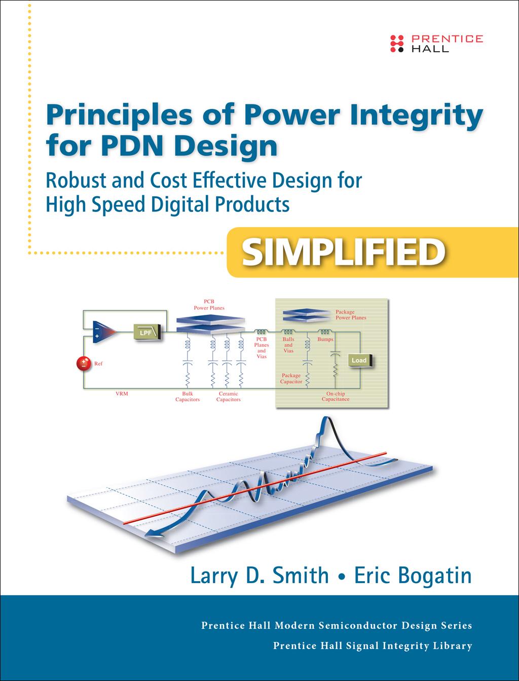
Between the VRM and die are interconnects on the package and board, which often carry discrete capacitors with their associated mounting inductance. The power distribution network (PDN) refers to all interconnects (usually inductive), the intentional energy storage devices (usually capacitive), and loss mechanisms (damping) between the VRM and the on-die Vdd-Vss power rails.
Power integrity is all about the quality of the power seen by the circuits on the die. What about noise created on the board power and ground planes by signals passing through cavities? Is this a signal integrity problem or a power integrity problem? Is the voltage noise generated by I/O switching currents and seen by the on-die Vcc and Vss rails a power integrity or signal integrity problem? Current that comes in through the common package lead inductance, which is ultimately connected to the VRM, generates this noise, which is sometimes referred to as switching noise or ground bounce.
This gray area between signal and power integrity has a profound impact on solutions that are offered for “ power integrity” problems. Adding decoupling capacitors on the board often provide a solution for reducing Vdd core noise but seldom improve the cavity noise induced by high bandwidth signals. In general, board-level capacitors offer little or no improvement to
return-plane bounce noise. In some cases, the parallel resonances they create can actually increase the cavityto-signal cross talk.
The first step to solving a problem is to clearly identify the problem and then correctly identify its root cause. A well-defined problem is often only a few steps away from a solution. Efficient solutions to problems are developed based on the actual root cause.
This book focuses on the specific power integrity problems related to noise on the Vdd rail, which powers the on-die core logic and enables it to perform functions. The gates powered by the on-die Vdd rail switch signals that communicate to other gates on the same die, and do not necessarily travel off die as I/O. Transient current caused by core activity causes noise on the Vdd rail, which is sometimes referred to as “self-aggression.” The principles, analysis methods, and recommended best design practices to minimize this problem can also apply to other signal integrity, power integrity, and EMI problems; however, the focus in this book is on selfaggression of the Vdd rail.
OTHER POWER INTEGRITY OR SIGNAL INTEGRITY PROBLEMS AND SOLUTIONS
The term “ power integrity” paints with too broad a brush to address all problems with general design recommendations. Instead, we need clear identification of the specific problem we are trying to solve, along with best design practices for each specific problem.
Some peripheral problems in a complete system design are sometimes categorized as power integrity:
• Noise on the Vcc-Vss rails from I/O switching, ground bounce, and switching noise: self-aggression by the Vcc rails
• Noise on the VRM output from its changing load impedance: self-aggression by the VRM
• Signal distortion as it travels through return path discontinuities: self-aggression by signals paths
• Noise from the power rails and VRM transferring onto and polluting the board-level PDN interconnects
• Cross talk between the voltage noise on the package and board-level PDN interconnects from all sources, coupling onto a Vdd rail
• Cross talk between the voltage noise on the package and board-level PDN interconnects from all sources, coupling to an I/O power rail
• Cross talk between the voltage noise on the package and board-level PDN interconnects and a signal which couples to the PDN
Each of these problems has a very different root cause and a different set of best design practices to reduce their impact. These topics are sometimes lumped under the signal integrity umbrella and sometimes the power integrity umbrella.
To avoid the possible confusion of assuming all power integrity problems are the same and hence one set of solutions apply to all problems engineers and designers should get in the habit of carefully articulating which problem is being addressed rather than using the general heading of power integrity or signal integrity.
A wealth of PDN design recommendations are offered in publications, at conferences, or by your favorite uncle. Blindly following any of them is dangerous. Unfortunately, many recommendations are either wrong or contradictory. This is partly because they are oriented toward only one of the specific problems listed above, but incorrectly generalized as the cure for all power integrity problems.
Be specific about the problem, the root cause, and the recommended best design practices.
MEETING THE CHALLENGE OF ROBUST PDN DESIGN
A poorly designed PDN can result in the product failing, usually at the worst possible time. PDN failures are difficult to diagnose because they are hard to reproduce.
Sometimes they result from a very specific combination of microcode running a specific set of problems. This makes it difficult to “test in the quality” of a PDN. A robust PDN must be designed in.
Some PDNs may actually be robust with no additional considerations on the board other than a low impedance VRM Other PDNs may require very specific combinations of capacitor values mounted in very specific positions, and then only run restricted microcode to be robust.
Every PDN is unique and has its own story. Each has its own combination of performance requirements, chip features, microcode, and design constraints on cost, performance, risk, and schedule. This makes it difficult to efficiently design a robust PDN by just following someone else’s best design principles. That’s where a solid design methodology plays an important role.
A common answer to many questions in any engineering field, including power integrity, is “…it depends.” The only way to answer “…it depends” questions is by clearly defining the problem and then putting in the numbers and performing analysis of the specific problem, the root cause, and the various solution options.
The most efficient design process for the PDN (and most aspects of high-performance product design) so that there is a high probability of “getting it right the first time” is based on four elements:
• Start with the established best design practices.
• Understand the essential principles of how signals interact with interconnects basically the principles of applied Maxwell’s Equations.
• Identify the common problems to avoid and their root causes.
• Leverage analysis tools to efficiently explore design space and find the appropriate cost-performance-
risk-schedule tradeoffs for each specific product’s details and constraints.
The goal for many projects is to find an acceptable design that meets the performance objectives at acceptable cost, risk, and schedule.
This book is designed to be a handbook for the practicing power integrity engineer to establish a firm foundation in the principles of power integrity, identify the root cause of the common problems found in PDN design, follow the best design practices, and perform engineering trade-off analysis to balance cost, performance, schedule, and risk.
WHO THIS BOOK IS REALLY FOR
As with all books in the Prentice Hall “Simplified” series, Principles of Power Integrity for PDN Design
Simplified minimizes the mathematical formalism to reveal the important engineering principles behind power integrity. If you are looking for detailed mathematical derivations and complicated numerical simulations, look elsewhere
This is not to say that mathematical rigor is not important every student of electrical engineering should have studied this in college. As a practicing engineer, being able to apply these principles to solve real problems is often more important than deriving every detail from Maxwell’s Equations.
This book is based on a specific design methodology for high-performance systems. The starting place is to use established best design principles Unfortunately, every design is custom, they each have their own story. They each have their own set of performance goals and cost, risk, and schedule constraints. This means you cannot blindly follow every design guideline, but must use your engineering judgement.
This does not mean grab your 3D full-wave simulator and simulate everything. This would be an incredibly
inefficient process with no guarantee of successfully converging on an acceptable solution.
The basis of engineering judgement is understanding the essential principles which are really applied Maxwell’s Equations identifying the problems to avoid and their root cause, and leveraging analysis tools to efficiently explore design space to find an acceptable answer. This book is a guideline for applying this methodology to designing robust PDN systems.
As two experts in the signal and power integrity fields, with more than 70 years of engineering experience between us, we have distilled into this book what we consider to be the most important engineering principles upon which power integrity engineering is based.
Our experience is based on having personally worked on many designs, helping many engineers, and having to rescue many failed designs. We’ve seen the consequence of carrying around misconceptions based on a recommendation from the person you sat next to on your last airplane flight who has a nephew who once built a board that worked so must have done it correctly.
Engineers involved in the design process must become their own expert and not rely on what the last expert they talked to said about a product that has nothing to do with the one they are currently working on.
Enough mathematics is included to accelerate a practicing engineer up the learning curve to immediately perform trade-off analysis and identify what is important and equally of value what is not important.
Equations are used as a shorthand to clarify which terms are important and how they combine to influence the result. They are used to restate the principle with more detail. They are the first line of attack when “putting in the numbers.”
Where possible, we show examples of simple simulations to illustrate the analytical approximations. Where appropriate, measurements from test vehicles and real systems are introduced to provide an anchor to
reality that these principles actually work, as long as they are applied with good engineering judgement.
If PDN design is in your future, you’ll find this book essential to your success.
FIVE FEATURES THAT MAKE THIS BOOK EASY TO NAVIGATE
To engineer a more efficient process for using this book, we ’ ve incorporated five valuable features.
As with all books in the Prentice Hall Simplified series, we ’ ve tried hard to take the complexity of realworld problems and break them down to their simplest form to identify the essential principles and how they apply. Approximations are included as a way of quantifying the principles and applying them to specific problem examples. They are a first step to help calibrate our engineering judgement so we can make sense of simulation results.
Where possible, the results of an analysis are shown graphically in figures. The figures with their extended captions tell a story in parallel with the text and equations.
In each section, we ’ ve pulled out what we consider to be some of the most important conclusions or observations as TIPS. These reinforce the section’s essences and make it easy when skimming the book to pick up or recall the highlights.
At the end of each chapter we ’ ve added “The Bottom Line” as a quick 10-point summary of the chapter’s most important points. After reading the chapter, the 10 points should be obvious and expected.
Finally, the PDN resonance calculator spreadsheet used extensively in the last chapter is available on the book’s companion web site at informit.com/title/9780132735551 and on the www.beTheSignal.com web site. Additional supplemental information on power integrity is available on these two web resource sites.
OUTLINE FOR THIS BOOK
Principles of Power Integrity for PDN Design
Simplified is organized as a training manual for the power integrity engineer to learn the strategies, tactics, essential principles, and skills for successful PDN design.
Chapter 1, “Engineering the Power Delivery Network,” provides a brief perspective on what the PDN is and why engineering a low impedance is so important. We introduce the idea of the impedance profile as an important design feature and indicator of PDN performance. We also introduce the most important figure of merit to describe the PDN design goal the target impedance. Our goal is to engineer a PDN impedance profile below the target impedance with acceptable cost, risk, and meet performance and schedule targets.
Chapter 2, “Essential Principles of Impedance for PDN Design,” provides a thorough review of impedance, which is the fundamental basis of evaluating a robust PDN. In particular, the properties of series and parallel RLC circuits are reviewed. These circuits determine the fundamental features of the PDN impedance profile. Simulation of the impedance profile of a collection of components is introduced as an essential skill. We show how any free version of a SPICE simulator can be used as an impedance analyzer.
Chapter 3, “Measuring Low Impedance,” introduces measurement techniques for low impedance. Typical PDN target impedances range from 1 Ω to lower than 1 mΩ. Special techniques are used to measure the very low impedance of components and the entire PDN ecology.
Chapter 4, “Inductance and PDN Design,” covers the essence of inductance, what it is, how it is affected by physical design, and how to estimate the loop inductance from physical design features. Engineering low loop inductance in the PDN interconnects is an important way to reduce peak impedances. When inductance cannot be
eliminated, it is important to know how much there is so that its impact can be evaluated.
Chapter 5, “Practical Multi-Layer Ceramic Chip Capacitor Integration,” reviews the properties of capacitors and how they behave individually and together. They are the primary component used to sculpt the impedance profile and manage the peaks. The five general tactics to reducing peak impedances from combinations of capacitors are introduced. In particular, the critical step of engineering low mounting inductance is introduced.
Chapter 6, “Properties of Planes and Capacitors,” introduces the properties of critically important power and ground planes in the PDN interconnect, and how the capacitors interact with the planes. The most important property of the planes the spreading inductance is explored in detail. In addition, we show that the plane cavity resonances are not important at all for the quality of power seen by die circuits
Chapter 7, “Taming Signal Integrity Problems When Signals Change Return Planes,” explores another function of PDN interconnects: to provide a low impedance for the signal return currents. Switching noise, a form of ground bounce, is a problem that results in noise on the planes when signals pass through them. This is the realm of signal integrity and is separate and distinct from power integrity. Because the root cause of switching noise is different from PDN noise on the core Vdd rails, the solutions are very different. We are careful to distinguish this important signal integrity problem from power integrity.
Chapter 8, “The PDN Ecology,” addresses the most important PDN feature: the peak impedance created by the on-die capacitance and the package lead inductance, and what can be done at the board level to reduce this peak. We show how to leverage all the design principles introduced up to this point to overcome the limitations created by this peak.
Chapter 9, “Transient Currents and PDN Voltage Noise,” describes the features of the current drawn by CMOS circuitry, and how this current spectrum interacts with the PDN impedance profile. Three important transient current waveforms are introduced: a clock-edge impulse, a step transient current, and a repetitive square wave of current. These waveforms interact with different PDN features. Most importantly, we show how the three elements impedance profile, transient current, and stimulated voltages all interact. Knowing any two elements enables us to evaluate the third.
Chapter 10, “Putting It All Together: A Practical Approach to PDN Design,” brings together all the principles and processes to illustrate how to design the specific features in the PDN to meet the performance goals. In particular, a simple spreadsheet–based analysis technique is introduced, which dramatically speeds up the process of creating a first-pass design. We walk through a few design scenarios and show an example of the power of the principles introduced in this book. From measured data, PDN parameters are developed that match measured performance incredibly well.
Larry Smith and Eric Bogatin January, 2017
Register your copy of Principles of Power Integrity for PDN Design
Simplified at informit.com for convenient access to downloads, updates, and corrections as they become available. To start the registration process, go to informit.com/register and log in or create an account.* Enter the product ISBN, 9780132735551, and click Submit. Once the process is complete, you will find any available content under “Registered Products.”
*Be sure to check the box that you would like to hear from us in order to receive exclusive discounts on future editions of this product.
Acknowledgments
The authors gratefully acknowledge the time and hard work of our reviewers who provided important comments and feedback on what worked and what didn’t in the initial draft. They helped to make this book more valuable to our readers Our thanks to Todd Hubing, Chris Padilla, Jay Diepenbrock, and Istvan Novak.