MaterialsandProcessesforNextGeneration Lithography1stEditionAlexRobinsonAndRichard Lawson(Eds.)
https://ebookmass.com/product/materials-and-processes-fornext-generation-lithography-1st-edition-alex-robinson-andrichard-lawson-eds/
Instant digital products (PDF, ePub, MOBI) ready for you
Download now and discover formats that fit your needs...
Next-Generation Solar Cells: Principles and Materials Yoon-Bong Hahn
https://ebookmass.com/product/next-generation-solar-cells-principlesand-materials-yoon-bong-hahn/
ebookmass.com
Dynamic Intentions: DCMC Next Generation (DreamCatcher MC
Next Generation Book 1) Liberty Parker
https://ebookmass.com/product/dynamic-intentions-dcmc-next-generationdreamcatcher-mc-next-generation-book-1-liberty-parker/
ebookmass.com
Next Generation Compliance: Environmental Regulation for the Modern Era Cynthia Giles
https://ebookmass.com/product/next-generation-complianceenvironmental-regulation-for-the-modern-era-cynthia-giles/
ebookmass.com
Soil Mechanics and Foundation Engineering 2nd Edition P Purushothama Raj
https://ebookmass.com/product/soil-mechanics-and-foundationengineering-2nd-edition-p-purushothama-raj/
ebookmass.com
How to Make Your Money Work: Decide what you want, plan to get there Eoin Mcgee
https://ebookmass.com/product/how-to-make-your-money-work-decide-whatyou-want-plan-to-get-there-eoin-mcgee/
ebookmass.com
Cicero's Academici libri and Lucullus: A Commentary with Introduction and Translations Tobias Reinhardt
https://ebookmass.com/product/ciceros-academici-libri-and-lucullus-acommentary-with-introduction-and-translations-tobias-reinhardt/
ebookmass.com
Surgical Critical Care And Emergency Surgery: Clinical Questions And Answers 3rd Edition Forrest "Dell" Moore (Editor)
https://ebookmass.com/product/surgical-critical-care-and-emergencysurgery-clinical-questions-and-answers-3rd-edition-forrest-dell-mooreeditor/
ebookmass.com
Diagnostic Imaging : Oral And Maxillofacial. 2nd Edition Lisa J. Koenig
https://ebookmass.com/product/diagnostic-imaging-oral-andmaxillofacial-2nd-edition-lisa-j-koenig/
ebookmass.com
Blackouts: A Novel Justin Torres
https://ebookmass.com/product/blackouts-a-novel-justin-torres/
ebookmass.com
https://ebookmass.com/product/advanced-nanostructures-forenvironmental-health-lucian-baia/
ebookmass.com
FrontiersofNanoscience SeriesEditor:RichardE.Palmer
TheNanoscalePhysicsResearchLaboratory, TheSchoolofPhysicsandAstronomy, TheUniversityofBirmingham,UK
Vol.1 NanostructuredMaterials editedby GerhardWilde
Vol.2 AtomicandMolecularManipulation editedby AndrewJ.MayneandGe ´ raldDujardin
Vol.3 MetalNanoparticlesandNanoalloys editedby RoyL.JohnstonandJ.P.Wilcoxon
Vol.4 Nanobiotechnology editedby JesusM.delaFuenteandV.Grazu
Vol.5 Nanomedicine editedby HuwSummers
Vol.6 Nanomagnetism:FundamentalsandApplications editedby ChrisBinns
Vol.7 NanoscienceandtheEnvironment editedby JamieR.LeadandEugeniaValsami-Jones
Vol.8 CharacterizationofNanomaterialsinComplexEnvironmental andBiologicalMedia editedby MohammedBaaloushaandJamieR.Lead
Vol.9 ProtectedMetalClusters:FromFundamentalstoApplications editedby TatsuyaTsukudaandHannuHakkinen
Vol.10 StructureandPropertiesofNanoalloys editedby RiccardoFerrando
Frontiersof Nanoscience MaterialsandProcessesfor NextGenerationLithography Volume11 Editedby
UniversityofBirmingham,Birmingham, UnitedKingdom
Milliken&Company,Spartanburg,SC, UnitedStates
AlexRobinson
RichardLawson
Elsevier
Radarweg29,POBox211,1000AEAmsterdam,Netherlands TheBoulevard,LangfordLane,Kidlington,OxfordOX51GB,UnitedKingdom 50HampshireStreet,5thFloor,Cambridge,MA02139,UnitedStates
Copyright © 2016ElsevierLtd.Allrightsreserved.
Nopartofthispublicationmaybereproducedortransmittedinanyformorbyanymeans, electronicormechanical,includingphotocopying,recording,oranyinformationstorage andretrievalsystem,withoutpermissioninwritingfromthepublisher.Detailsonhowto seekpermission,furtherinformationaboutthePublisher’spermissionspoliciesandour arrangementswithorganizationssuchastheCopyrightClearanceCenterandthe CopyrightLicensingAgency,canbefoundatourwebsite: www.elsevier.com/permissions
Thisbookandtheindividualcontributionscontainedinitareprotectedundercopyrightby thePublisher(otherthanasmaybenotedherein).
Notices Knowledgeandbestpracticeinthisfieldareconstantlychanging.Asnewresearchand experiencebroadenourunderstanding,changesinresearchmethods,professional practices,ormedicaltreatmentmaybecomenecessary.
Practitionersandresearchersmustalwaysrelyontheirownexperienceandknowledgein evaluatingandusinganyinformation,methods,compounds,orexperimentsdescribed herein.Inusingsuchinformationormethodstheyshouldbemindfuloftheirownsafety andthesafetyofothers,includingpartiesforwhomtheyhaveaprofessionalresponsibility.
Tothefullestextentofthelaw,neitherthePublishernortheauthors,contributors,or editors,assumeanyliabilityforanyinjuryand/ordamagetopersonsorpropertyasa matterofproductsliability,negligenceorotherwise,orfromanyuseoroperationofany methods,products,instructions,orideascontainedinthematerialherein.
LibraryofCongressCataloging-in-PublicationData
AcatalogrecordforthisbookisavailablefromtheLibraryofCongress
BritishLibraryCataloguinginPublicationData
AcataloguerecordforthisbookisavailablefromtheBritishLibrary
ISBN:978-0-08-100354-1
ISSN:1876-2778
ForinformationonallElsevierpublicationsvisit ourwebsiteat https://www.elsevier.com
Publisher: JoeHayton
AcquisitionEditor: SimonHolt
EditorialProjectManager: SabrinaWebber
ProductionProjectManager: MohanambalNatarajan
CoverDesigner: AlanStudholme
TypesetbyTNQBooksandJournals
Contributors PanagiotisArgitis
InstituteofNanoscienceandNanotechnology,NationalCenterforScientific Research“Demokritos”,Athens,Greece
StuartA.Boden
ElectronicsandComputerScience,FacultyofPhysicalSciencesand Engineering,UniversityofSouthampton,Southampton,UnitedKingdom
ElizabethBuitrago
PaulScherrerInstitute,VilligenPSI,Switzerland
BrianCardineau
InpriaCorporation,Corvallis,OR,UnitedStates
GuyA.DeRose
KavliNanoscienceInstitute,CaliforniaInstituteofTechnology,Pasadena,CA, UnitedStates
YasinEkinci
PaulScherrerInstitute,VilligenPSI,Switzerland
RobertoFallica
PaulScherrerInstitute,VilligenPSI,Switzerland
AndreasFrommhold
SchoolofChemicalEngineering,UniversityofBirmingham,Birmingham, UnitedKingdom
MarcusKaestner
DepartmentofMicro-andNanoelectronicSystems,InstituteofMicro-and Nanoelectronics,FacultyofElectricalEngineeringandInformationTechnology, IlmenauUniversityofTechnology,Ilmenau,Germany
DouglasA.Keszler
DepartmentofChemistry,OregonStateUniversity,Corvallis,OR,UnitedStates; InpriaCorporation,Corvallis,OR,UnitedStates
YanaKrivoshapkina
DepartmentofMicro-andNanoelectronicSystems,InstituteofMicro-and Nanoelectronics,FacultyofElectricalEngineeringandInformationTechnology, IlmenauUniversityofTechnology,Ilmenau,Germany
TeroS.Kulmala
SwissLithoAG,Zurich,Switzerland
RichardA.Lawson
ResearchDivision,Milliken&Company,Spartanburg,SC,UnitedStates
ScottM.Lewis
SchoolofChemistry,TheUniversityofManchester,Manchester,UnitedKingdom
PatrickNaulleau
CenterforX-rayOptics,LawrenceBerkeleyNationalLaboratory,Berkeley,CA, UnitedStates
DimitraNiakoula
HeliospheraS.A.,Tripolis,Greece
D.FrankOgletree
MolecularFoundry,LawrenceBerkeleyNationalLaboratory,Berkeley,CA, UnitedStates
DeirdreOlynick
MolecularFoundry,LawrenceBerkeleyNationalLaboratory,Berkeley,CA, UnitedStates
PhilipC.Paul SwissLithoAG,Zurich,Switzerland
IvoW.Rangelow
DepartmentofMicro-andNanoelectronicSystems,InstituteofMicro-and Nanoelectronics,FacultyofElectricalEngineeringandInformationTechnology, IlmenauUniversityofTechnology,Ilmenau,Germany
AlexP.G.Robinson
SchoolofChemicalEngineering,UniversityofBirmingham,Birmingham, UnitedKingdom
AdamSchwartzberg
MolecularFoundry,LawrenceBerkeleyNationalLaboratory,Berkeley,CA, UnitedStates
XiaoqingShi
ElectronicsandComputerScience,FacultyofPhysicalSciencesand Engineering,UniversityofSouthampton,Southampton,UnitedKingdom
JamesW.Thackeray
DowElectronicMaterials,Marlborough,MA,UnitedStates
WillemF.vanDorp
DepartmentofImagingPhysics,DelftUniversityofTechnology,Delft, TheNetherlands
VeronikiP.Vidali
InstituteofNanoscienceandNanotechnology,NationalCenterforScientific Research“Demokritos”,Athens,Greece
AndrewK.Whittaker
AustralianInstituteforBioengineeringandNanotechnology,Universityof Queensland,StLucia,QLD,Australia
DongxuYang
SchoolofPhysicsandAstronomy,UniversityofBirmingham,Birmingham, UnitedKingdom
Preface Themodernworldisthoroughlypopulatedwithintegratedcircuits(ICs)andother microelectronicdevices.Theubiquityofthesedeviceshascomeaboutbecausetheir computingpowerhasincreasedexponentiallyovertime,whileatthesametimethe costpercomputingpowerhasdroppedduetoshrinkingthesizesofthetransistors. Theshrinkinfeaturesizeshasbeenenabledinalargemeasurebyadvancementsin lithography,whichisthetechniqueusedtoprintthecircuitfeaturesonsiliconwafers duringICfabrication.Thecriticalpiecesrequiredforscalingareboththematerials andtheprocessesusedforlithography.
Currentlythereissignificantworldwideresearcheffortbothindustriallyandin academiaintonext-generationlithographyprocessessuchasEUV,advanced e-beam,nanoimprint,scanningprobe,andionbeamlithography.Thereislikewise similareffortinbotharenasintonext-generationmaterialsforlithographyincluding numerousnovelapproachestoresistchemistryandingeniousextensionsoftraditionalphotopolymers.Thisbookthereforeaimstobringtogethersomeofthe world’sforemostlithographicdevelopmentscientistsfromthevariouscommunities toproduceinoneplaceacompletedescriptionofthemanyapproachestolithographicmaterialsandprocessdesign,development,andcharacterization.
Resistchemistryfornext-generationlithographyislikelytobequitedistinctfrom thewell-knownprocessofphotochemistryincurrentuse.Fornoncontactmethodsthe actinicradiationunderconsiderationistypicallyfarmoreenergetic.Thisisdiscussed in Chapter1 togetherwithabriefintroductiontoresistchemistryinEUVandelectronbeamlithography,alongsideareviewofcurrentresistprocesses.In Chapter2, newinsightsintothemechanismsofEUVresistradiationchemistryarepresented fromtheperspectiveofanexaminationofthefundamentalinteractionsofsoft X-rayswithmatter,photoionization,andmolecularrelaxationprocesses.In Chapter 3,theexaminationoftheEUVresistmechanismisextendedfurtherviaadetailed analysisoftheinteractionsoflowenergyelectronsintheresistfilm,identifyingthe manyproductive(andnonproductive)reactionpathwaysavailable.
Chapters4and5investigatetheprocessandpatterningchallengesfacingEUV lithography themostlikelynext-generationcontender.In Chapter4,readersare introducedtothetechniqueofEUVinterferometriclithography,whichhasbeen usedtogeneratemanyoftheexperimentalresultsseeninlaterchapters.General resistmaterialchallengesarethenexaminedandpotentialstrategiesdiscussed. Chapter5 introducesEUVopticallithography usingamaskratherthanagrating forpatterngeneration andadetailedanalysisofthetoolchallengesfacedbyindustry.OneofthemostsignificantproblemsinEUVlithographyrelatestostochastic variations,andthischapterintroducesanewmodeltosimulatetheseeffectsand identifyareasofmostconcern.Finallytheprogressincommercialandresearch resistsexposedonamask-basedEUVtoolisreviewed.
Chapters6 13addressresistchemistry. Chapter6 presentsprogressinresists thatoperateviaamechanismofchainscission.Thesearetypicallyknownas
nonchemicallyamplifiedresists.Whilesuchsystemsaretypicallyconsideredtobe quiteinsensitive,newworkonhigh-speedvariantsispresented.ChemicallyamplifiedsystemsforEUVlithographyarereviewedin Chapter7.Whilemanychemicallyamplifiedsystemsareproprietary,andresultsintheliteratureoften presentedwithoutsignificantchemicaldetail,thischapterseekstoidentifythemajor recenttrendsinchemicallyamplifiedsystems.
Todatethemajorityofresistsystemshavebeenbasedonpolymericmaterials. However,inthelasttwodecadesasignificantamountofresearchintomolecularresist systemshasbeenundertaken. Chapter8 examinesawidevarietyofnegativetone molecularresistsystems,primarilybutnotexclusivelyoperatingviacross-linking mechanisms,while Chapter9 looksatpositivetonemolecularresistsystems,via, forinstance,solubilityswitchmechanisms.Anotherrecentalternativetopolymeric resistsareinorganicresists. Chapter10 introducestothemostwidelyusedofthe inorganicsystems,hydrogensilsesquioxane(HSQ).Theexposuremechanismis radicallydifferenttothatoforganicsystemsandisexplainedindepth,together withareviewofprocessing. Chapter10 alsoaddressesanexcitingnewmaterial class high-Znanoclusterresists,examinedviatheprototypicalhafniumperoxide sulfate.Thesedepartinalmosteverywayfromthetraditionalparadigmofaphotoresist,butnonethelesshavedemonstratedoutstandingperformance.Anothernovel approachthatutilizesorganometalliccomplexesispresentedin Chapter11.By selectingmetalatomsofhighEUVabsorbancetogetherwithappropriateligandsto enablespincoating,anddevelopment,anumberofhigh-speedEUVresistshave beendemonstrated.
Chapter12 takesafundamentallydifferentapproachtoresistdevelopment. AmaterialinitiallydevelopedtodemonstratehighopacityintheUV,soastoallow itsuseasanelectron-beamwritablephotomaskispresented.Goodresultsasa photomaskareindeeddemonstrated,buttheresisthasalsobeenfoundtoenable astonishinglyhigh-aspectratioelectronbeampatterning,primarilyduetothevery low-densitynatureofthefilm.Filmdensityissomethingthatisrevisitedin Chapter 13,aspartofanexaminationofaselectionoftheothernovelapproachesthathave beenundertakenrecently.
Thelastsectionofthebookaddressesseveralnewapproachestonext-generation lithography.WhileEUViscoveredextensivelyacrossthefirst13chapters,various otherapproachesarealsounderdevelopment. Chapter14 presentsashortreviewof thechallengesandpotentialsolutionsofnext-generationlithography.In Chapter 15,thetopicofscanningprobelithographyisexaminedingreatdepth,before focusingonelectricalfieldinteractionsofananoprobewithresist,andapproaches toscanningprobelithographythroughputenhancement. Chapter16 dealswith thermalscanningprobelithographyandintroducesthenewcommercialthermal probetooltheNanoFrazor,fromSwisslitho.Finallyin Chapter17,therecentdevelopmentoftheScanningHeliumIonBeamLithographytoolanditsapplicationto nanolithographyisdiscussed.
AlexP.G.RobinsonandRichardA.Lawson
Acknowledgments WewouldliketothankProfessorRichardPalmer,theserieseditorof Frontiersin Nanoscience,fortheopportunitytoworkonthisprojectthatseekstocompileathoroughdescriptionofthemanycurrentapproachestolithographicmaterialsandprocessdesign.Wewouldalsoliketothankallourcolleagueswhosehardworkwriting thechaptersmadethisbookpossible.AgreatdealofthanksgoestoSabrinaWebber, theeditorialprojectmanageratElsevier,whowascriticallyhelpfulthroughtheend oftheprocessandwasexceedinglypatientasweslowlydeliveredallthevarious partsofthebook.InadditiontoSabrina,HannahColfordandDerekColeman wereofgreathelpaseditorialprojectmanagersinvariousearlierstagesoftheprocessandwereparticularlyhelpfulaswegottheprojectofftheground.Additional thanksalsogotootherpeopleatElsevier,includingSimonHolt,SusanDennis, MohanambalNatarajan,andmanymoreworkingbehindthescenes.Finally,we wouldespeciallyliketothankourfamilieswhowereexceptionallypatientwith allthelonghoursputintowritingandeditingandwithoutwhosesupporttheproject wouldnothavebeencompleted.
AlexP.G.RobinsonandRichardA.Lawson
Listofabbreviations AAAcidamplifier
ADAdamantylester
AEVEAdamantylethylvinylether
AFMAtomicforcemicroscopy
AILAchromaticinterferencelithography
ASITPA4,40 ,400 -tris(Allylsuccinimido)triphenylamine
ATLAchromaticTalbotlithography
BCMTPB1,3,5-tris[4-(Tert-butoxycarbonylmethoxy)phenyl] benzene
BCPsBlockcopolymers
BEBindingenergy
BEsBackscatteredelectrons
BPY2,20 -Bipyridine
BZABenzoicacid
CAChemicalamplification
CARsChemicallyamplifiedresists
CDCriticaldimension
b-CD
b-Cyclodextrins
CMC(n)AOMep-Chloromethylmethoxycalyx[n]arenemolecule
CVDChemicalvapordeposition
DBU1,8-Diazabicycloundec-7-ene
DCTDoseCalibrationTool
DDRMDrydeveloprinsematerial
DDRPDrydevelopmentrinseprocess
DEADissociativeelectronattachment
DIDissociativeionization;Dissolutioninhibitor
DNQDiazonaphthoquinone
DOFDepthoffocus
DPI-TsDiphenyliodoniumtosylate
DPNDip-pennanolithography
DSADirectedself-assembly
DUVDeepultraviolet
E-beamElectronbeam
EBLElectronbeamlithography
EMAX Doseformaximumfilmthicknessretention
ENEthylenediamine
ESIZE Sizingdose
ESRspectroscopyElectronspinresonancespectroscopy
ETMDElectrontransferemediateddecay
EUVExtremeultraviolet
EUVresistExtremeultravioletresist
EUV-ILExtremeultravioletinterferencelithography
EUVLExtremeultravioletlithography
FBMPoly(hexafluorobutylmethacrylate)
fccFace-centered-cubic
FEFieldevaporation
FE-SPLFieldemissionSPL
FEBIDFocusedelectronbeam-induceddeposition
FEBIPFocusedelectronbeam-inducedprocessing
FIBlithographyFocusedionbeamlithography
FTIRFourier-transforminfrared
GFISGasfieldionsource
GPCGelpermeationchromatography
HFHydrofluoricacid
HIBLHeliumionbeamlithography
HIMHeliumionmicroscope
HMDSHexamethyldisilazane
HOMOHighestoccupiedmolecularorbital
HPlinesHalf-pitchlines
HPVEHyperlactylvinylether(1-vinyloxy-4-oxatricyclo [4.1.13.8]undecane-5-on)
HSQHydrogensilsesquioxane
HVMHigh-volumemanufacturing
IBLIon-beamlithography
ICDIntercoulombicdecay
ICsIntegratedcircuits
ILInterferencelithography
ILSImagelogslope
IMFPInelasticmeanfreepath
IPAIsopropanol
ITRSInternationalTechnologyRoadmapforSemiconductors
KOHPotassiumhydroxide
LAOLocalanodicoxidation
LELELitho-Etch-Litho-Etch
LERLine-edgeroughness
LUMOLowestunoccupiedmolecularorbital
LWRLine-widthroughness
MAAMethacrylicacid
MCBMonochlorobenzene
MCNMethacrylonitrile
MFSMinimumfeaturesize
MGMolecularglass
MIBKMethylisobutylketone
ML2Masklesslithography
MOREMolecularorganometallicresists
MPPMMultivariatePoissonpropagationmodel
NANumericalaperture
NCAresistsNonchemicallyamplifiedinorganicresists
NDNeutraldissociation
NGLNext-generationlithography
NILNanoimprintlithography
NILmethodNanoimprintmethod
NILSNormalizedILS
NMRNuclearmagneticresonance
NRTNormalizedremainingthickness
NTDNegative-tonedevelopment
ODOpticaldensity
OOBradiationOut-of-bandradiation
PABPost-applicationbake
PAGPhotoacidgenerator
PBMSPly(butylmethylsilane)
PBPresistsPolymer-boundPAGresists
PBSPoly(1-butenesulfone)
PDAPhotodestructiveanion;Photodestructiveacid
PDBsPhotodecomposablebases
PDMSPoly(dimethylsiloxane)
PDNPhotodecomposablenucleophile
PEBPost-exposurebake
PECProximityeffectcorrection
PGMEPropyleneglycolmethylether;Propyleneglycol monomethylether
PGMEAPropyleneglycolmethyletheracetate
PHEMAPoly(2-hydroxyethylmethacrylate)
PHOSTPolyhydroxystyrene
PHSPolyhydroxystyrene
D,L-PLAPoly(D,L-lacticacid)
L-PLAPoly(L-lacticacid)
PMGIPolymethylglutarimide
PMMAPolymethylmethacrylate
PMPSPoly(methylphenylsilane)
POSSPolyhedraloligomericsilsesquioxane
PPAPolyphthalaldehyde
PS-b-PDMSPolystyrene-block-polydimethylsiloxane
CHAPTER Overviewofmaterialsand processesforlithography 1 RichardA.Lawson*, 1,AlexP.G.Robinsonx *ResearchDivision,Milliken&Company,Spartanburg,SC,UnitedStates xSchoolofChemicalEngineering,UniversityofBirmingham,Birmingham,UnitedKingdom 1Correspondingauthor:E-mail:richard.lawson@milliken.com
CHAPTEROUTLINE 1.1Introduction.........................................................................................................2
1.2OverviewofLithographyProcess...........................................................................5
1.3LithographicExposureSourcesandProcesses.......................................................7
1.3.1UltravioletLithography........................................................................7
1.3.2DUVLithography 248nmand193nm,Immersion,andMultiple Patterning..........................................................................................8
1.3.3ExtremeUltravioletLithography.........................................................12
1.3.4E-BeamLithography.........................................................................13
1.3.5OtherLithographyProcesses IonBeam,ScanningProbe,and Nanoimprint....................................................................................15
1.4CharacterizationandFiguresofMeritforResists.................................................18
1.5ResistMaterialsandChemistry...........................................................................26
1.5.1NonchemicallyAmplifiedResists.......................................................26
1.5.2ChemicallyAmplifiedResists............................................................28
1.5.3ResistPhysicalPropertiesandEtchResistance..................................31
1.5.4PhotoacidGeneratorChemistryandPhysics........................................33
1.5.5MolecularResistsandInorganicResists.............................................38
1.6ChallengesinModernResistDesign....................................................................44
1.6.1ExposureStatisticsandShotNoise....................................................45
1.6.2PhotoacidDiffusion..........................................................................46
1.6.3Resolution,LineEdgeRoughness,andSensitivityTrade-off.................51
1.6.4PatternCollapse...............................................................................54
1.7Conclusions.......................................................................................................60 References...............................................................................................................61
1.1 INTRODUCTION Themodernworldisthoroughlypopulatedwithintegratedcircuits(ICs)andother microelectronicdevices.Thesedevicesarepresentinallaspectsofsocietyandare integraltotherunningofgovernment,business,healthcare,transportation,security, andevendomestictasks.Oncefoundprimarilyincomputers,ICsarenowpervasive inalmosteverythingoneinteractswith,includingcellphones,automobiles,televisions,toys,evenappliancessuchasrefrigeratorsandcoffeemakers.Theyhave changedthewaypeoplework,play,andcommunicate.Theubiquityofthesedevices hascomeaboutbecausetheircomputingpowerhasincreasedexponentiallyover time,whileatthesametimethecostpercomputingpowerhasdropped.ThisperformanceandcosthasbeenenabledbytheabilityoftheICmanufacturerstodoublethe numberoftransistorsperchiproughlyeverytwoyears.1 Thistrendiscommonly referredtoasMoore’sLaw.2,3 GordonMooreobservedthistrendin1965,andhe predictedthisscalingwouldcontinueforanotherdecade.Itcontinuednotonly foranotherdecade,butithascontinuedforover50years.Itstartedasanobservation onscaling,butthenbecameanindustrymandate.
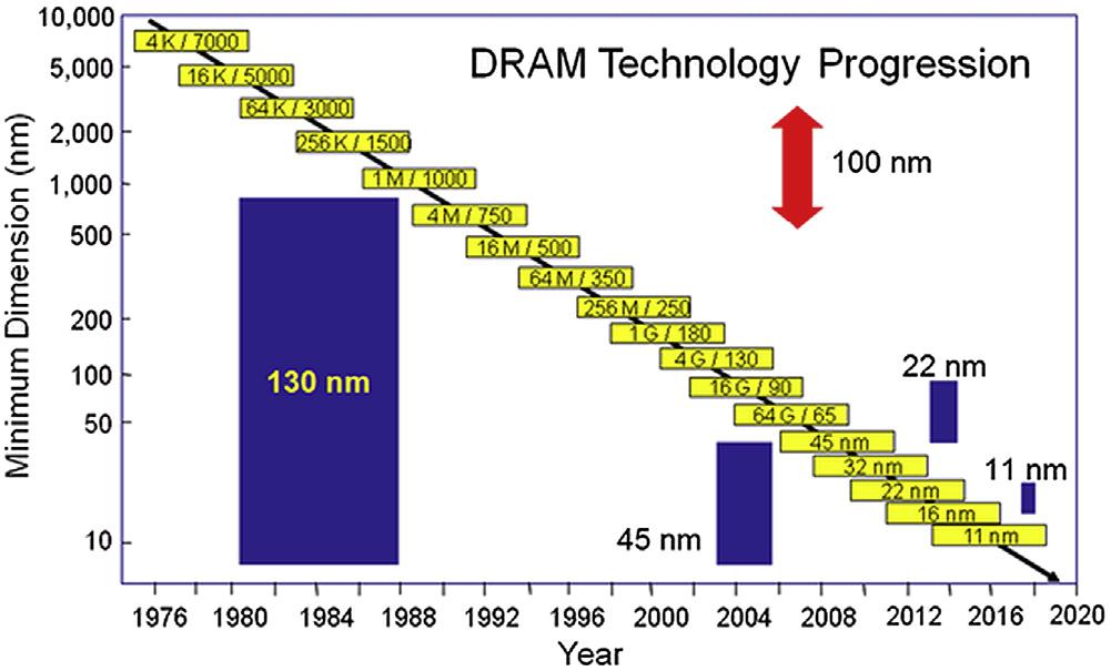
Thedoublingofthenumberoftransistorsperchiphasbeendonebyshrinking thesizesofthetransistors.Theshrinkinfeaturesizeshasbeenenabledinalarge measurebyadvancementsinlithography,whichisthetechniqueusedtoprintthe circuitfeaturesonsiliconwafersduringICfabrication.4 Avisualexampleofthe scaleofshrinkisshownin Fig.1,whichshowsthetransistordimensionrequired tomaintainMoore’slawalongwithacrosssectionofthephotoresistpattern
FIGURE1
TransistordimensionrequiredtomaintainMoore’slaw.The darkrectangles showthescaling ofthephotoresistpatternheightandwidthrequiredtoproducethesetransistordimensions. ReproducedfromLawsonRA,2011. Molecularresistsforadvancedlithography design,synthesis, characterization,andsimulation [Ph.D.dissertation].Atlanta,GA:GeorgiaInstituteofTechnology. http://hdl.handle.net/1853/39601
requiredtoproducethesedimensions.5 Photoresistsaretheradiation-sensitivematerialsusedforformingthereliefpatternsrequiredtobuildupICdevices.Asshown in Fig.1,transistorshavecontinuedtoshrinktowherecurrentfeaturesizesaresub20-nm,andsub-10-nmfeaturesareonlyafewyearsaway.Asfeaturesrapidly approachmolecularandevenatomiclengthscales,anumberoftechnologicalchallengeshavearisenthatthreatentohaltthissteadyprogress,andthustheentireIC industry.
Thecriticalpiecesrequiredforscalingareboththematerialsandtheprocesses usedforlithography.Currentlythereissignificantworldwideresearcheffortboth industriallyandinacademiaintonext-generationlithographyprocessessuchas extremeultraviolet(EUV),advancede-beam,nanoimprint,scanningprobe,and ionbeamlithography.Thereislikewisesimilareffortinboththeindustrialand theacademiclithographyarenasintonextgenerationmaterialsforlithography includingnumerousnovelapproachestoresistchemistryandingeniousextensions oftraditionalphotopolymers.Thisbookthereforeaimstobringtogethersomeofthe world’sforemostlithographicdevelopmentscientistsfromthevariouscommunities toproduceinoneplaceacompletedescriptionofthemanyapproachestolithographicmaterialsandprocessdesign,development,andcharacterization.Resist chemistryfornext-generationlithographyislikelytobequitedistinctfromthe well-knownprocessofphotochemistryincurrentuse.Fornoncontactmethods, theactinicradiationunderconsiderationistypicallyfarmoreenergetic.Thiswill bediscussedin Section1.3 ofthischapter,togetherwithabriefintroductiontoresist chemistryinEUVandelectronbeamlithography,alongsideareviewofcurrentresist processes.InChapter2,newinsightsintothemechanismsofEUVresistradiation chemistryarepresentedfromtheperspectiveofanexaminationofthefundamental interactionsofsoftX-rayswithmatter,photoionization,andmolecularrelaxation processes.Theseprocessescanleaddirectlytochemistrynotpresentatlongerwavelengths,butalsototheproductionoflowenergyelectronswhichareimportantfor EUVresists.InChapter3theexaminationoftheEUVresistmechanismisextended furtherviaadetailedanalysisoftheinteractionsoflowenergyelectronsintheresist film,identifyingthemanyproductive(andnonproductive)reactionpathways available.
Chapters4and5investigatetheprocessandpatterningchallengesfacingEUV lithography themostlikelynextgenerationcontender.Chapter4introducesthe techniqueofEUVinterferometriclithography,whichhasbeenusedtogenerate manyoftheexperimentalresultsseeninlaterchapters.Generalresistmaterialchallengesarethenexaminedandpotentialstrategiesarediscussed.Chapter5introduces EUVlithographywhichusesmoreconventionaloptics,i.e.,usingamaskandprojectionopticsratherthanagratingforpatterngeneration,andadetailedanalysisof thetoolchallengesfacedbyindustry.OneofthemostsignificantproblemsinEUV lithographyrelatestostochasticvariations,bothduetothehighenergyperphoton, andthuslowphotonnumberperdose,butalsothevariabilityofmulticomponent resistmaterialspushedtothelimitsoftheirperformance.Chapter5introducesa newmodeltosimulatetheseeffectsandidentifyareasofmostconcern.Finally
theprogressincommercialandresearchresistsexposedonamask-basedEUVtool isreviewed.
FromChapter6onward,thebookaddressesresistchemistry.Thefirstofthese chapterspresentsprogressinresiststhatoperateviaamechanismofchainscission. Thesearetypicallyknownasnonchemicallyamplifiedresists,asoneexposureevent leadstoasinglechemicaleventintheresist.Whilesuchsystemsaretypically consideredtobequiteinsensitive,newworkonhigh-speedvariantsispresented. ChemicallyamplifiedsystemsforEUVlithographyarereviewedinChapter7. Whilemanychemicallyamplifiedsystemsareproprietary,andresultsintheliteratureoftenpresentedwithoutsignificantchemicaldetail,thischapterseekstoidentify themajorrecenttrendsinchemicallyamplifiedsystems.
Todatethemajorityofresistsystemshavebeenbasedonpolymericmaterials. However,inthelasttwodecadesasignificantamountofresearchintomolecular resistsystemshasbeenundertaken.Chapter8examinesawidevarietyofnegativetonemolecularresistsystems,primarilybutnotexclusivelyoperatingviacrosslinkingmechanisms,whileChapter9looksatpositive-tonemolecularresistsystems, via,forinstance,solubilityswitchmechanism(see Section1.2 ofthischapterfora discussionofresisttone).Anotherrecentalternativetopolymericresistsareinorganic resists.Chapter10introducesthemostwidelyusedoftheinorganicsystems, hydrogensilsesquioxane(HSQ).Theexposuremechanismisradicallydifferentto thatoforganicsystemsandisexplainedindepth,togetherwithareviewofprocessing.Chapter10alsoaddressesanexcitingnewmaterialclass:high-Z nanoclusterresists,examinedviatheprototypicalhafniumperoxidesulfate(HafSOx).Thesedepart inalmosteverywayfromthetraditionalparadigmofaphotoresist,butnonetheless havedemonstratedoutstandingperformance.Anothernovelapproachutilizing organometalliccomplexesispresentedinChapter11.Byselectingmetalatomsof highEUVabsorbancetogetherwithappropriateligandstoenablespincoatingand development,anumberofhigh-speedEUVresistshavebeendemonstrated.
Chapter12takesafundamentallydifferentapproachtoresistdevelopment.A materialinitiallydevelopedtodemonstratehighopacityintheUV,soastoallow itsuseasanelectronbeamwritablephotomaskispresented.Goodresultsasaphotomaskareindeeddemonstrated,butserendipitouslytheresisthasalsobeenfoundto enableastonishinglyhighaspectratioelectronbeampatterning,primarilyduetothe verylow-densitynatureofthefilm.Electronbeampatterningresistfeatureswith aspectratiosfarbeyondanythingthatcouldbeachievedinotherresistsareshown. FilmdensityissomethingthatwillberevisitedinChapter13,aspartofanexaminationofaselectionoftheothernovelapproachesthathavebeenundertaken recently.ThechapteraddressesnovelapproachestoEUVlithography,including lowandhighabsorbancyfilmsandnovelnanoparticle-basedresists.
Thelastsectionofthebookaddressesseveralnewapproachestonext-generation lithography.WhileEUViscoveredextensivelyacrossthefirst13chapters,various otherapproachesarealsounderdevelopment.Chapter14presentsashortreviewof thechallengesandpotentialsolutionsofnext-generationlithography.InChapter15, thetopicofscanningprobelithographyisexaminedingreatdepth,beforefocusing
onelectricalfieldinteractionsofananoprobewithresist,andapproachestoscanning probelithographythroughputenhancement.Chapter16dealswiththermalscanning probelithographyandintroducesthenewcommercialthermalprobetooltheNanoFrazorfromSwisslitho.FinallyinChapter17,therecentdevelopmentofthescanning heliumionbeamlithographytoolanditsapplicationtonanolithographyisdiscussed.
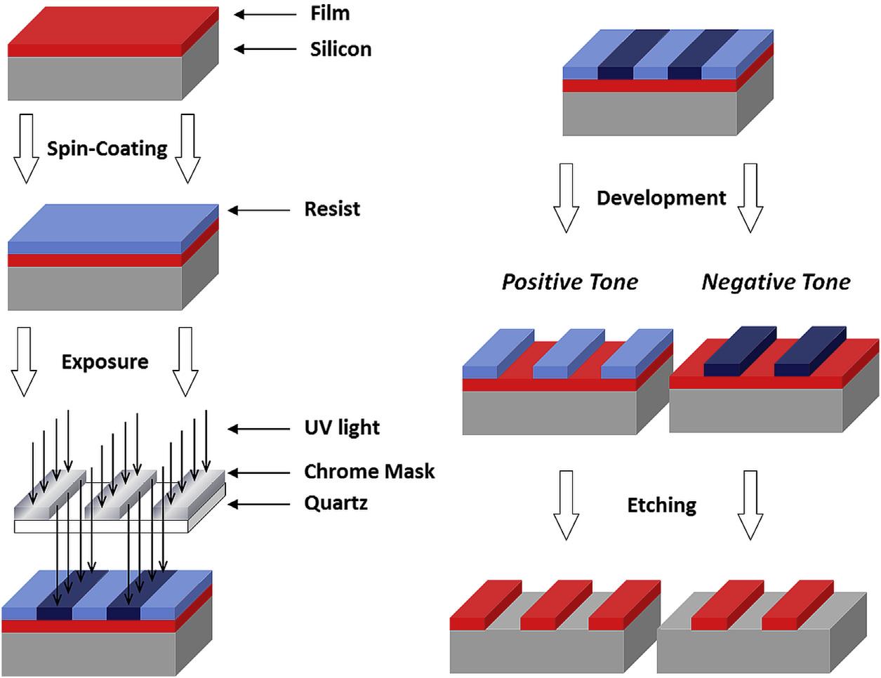
1.2 OVERVIEWOFLITHOGRAPHYPROCESS Lithographyistheartandscienceofproducingapatternonasubstrate.Thetermis usedmostoftentodayinconnectionwithsemiconductorprocessing.Additionaladjectivesareoftenusedtomorespecificallydefinethetechniquesuchasoptical lithographyorphotolithography(usingUVlighttogeneratethepatterns),imprint lithography(amoldispressedorimprintedintoamaterialtogeneratethepatterns), e-beamlithography(electronbeamsareusedtogeneratethepattern),orEUVlithography.Themostcommonlyusedformoflithographyinhighvolumemanufacturing isopticallithographyandageneralizedoverviewoftheprocessisshownin Fig.2.
Ahighlysimplifieddescriptionoftheprocessisasfollows.Thesubstrate(usuallyasiliconwafer)isusuallycoatedwithathinfilmofafunctionalmaterialora multilayerstackofmaterialsthatcouldserveanynumberofrolessuchaslow-kor high-kdielectric,etch-resistanthardmask,orconductinglayer.Photoresist,whichis aphotosensitivematerialthatistypicallycomposedmostlyofanorganicpolymer,is thenspincoatedontothefilmstack.Thetermphotoresistisoftenshortenedsimply toresistwhichisalsoamoregeneraltermforthesetypesofmaterials;especially sinceresistsformanyalternativeandfutureexposuresourceswouldnotbeexposed tophotonsbutratherelectrons,ions,orotherphysicalsourcesofapattern.
UVlightisthenshonethroughamask,whichselectivelyallowslightthrough certainregionstogenerateapatternontheresist.Themaskhashistoricallybeen madeofquartzwithchromepatternsontopthatcontrolwherethelightshinesthrough themask.TheradiationpatternfromtheUVlightinduceschemicalchangesinthe resist,whichselectivelymodifiesthesolubilityoftheexposedregionsinaliquid calleddeveloper.Thewaferiscommonlybakedafterthisexposurestep[calledapostexposurebake(PEB)]tofurtherinducechemicalchangeintheexposedregions.
Thedevelopmentstepisnext,andiswheredeveloperispouredorsprayedonto theresistandcertainregionsoftheresistaredissolved,whileotherregionsremain onthewafer.Theexposedregionswilleitherbedissolvedorremaindependingon thetoneoftheresist.Positive-toneresistsarethosewheretheexposedareasaredissolvedduringdevelopment;thesolubilitychangeisoftenduetochemistrythatoccursduringexposureorinthePEBwhichchangesthepolarityorfunctionalgroups oftheresist.Negative-toneresistsarethosewheretheexposedregionsarenotdissolvedduringdevelopmentandtheexposedareasaredissolvedinstead.Solubility changeinthesematerialscanlikewiseoccurbymanydifferentmethods,although twoofthemostcommonarecross-linkingtoformhighmolecularweightnetwork structuresandchangesinfunctionalgroupsoftheresistwhichaffectpolarity.
Generalizeddiagramoftheopticallithographyprocess.Theprocessstartsinupperleftand goestop-to-bottomandthentherightsidetop-to-bottom.Resistisspincoatedontoa substrateconsistingofasiliconwaferandotherdepositedfilms.Theresistispatterned throughamasktoselectivelyexposeareasontheresistandthenthewaferiscommonly bakedonahotplate.Developmentgeneratesthethree-dimensionalreliefpatterninthe resistandthatpatternistransferredintothesubstratethroughanetchprocess.
Finally,theremainingpatterninthedevelopedresististransferredintotheunderlyingfilmstackusinganetchprocess.Thisetchprocesscouldbeawetorchemicaletchwhereliquidchemicalsselectivelyremovetheunderlayer(UL)while havingaminimaleffectontheremainingphotoresist.However,itismorecommon thattheetchingisdoneusingplasmaetchingwherehighenergyparticlesselectively etchtheULcomparedtotheremainingresist.Plasmaetchingallowsahighlevelof controlandselectivityatboththenanoscaleandwafersizescalebychangingthe variousparametersintheetchchambersuchasetchgasesandspecies,voltage, biasonthewafer,pressure,andlocalwafertemperature,amongmanyothers.By controllingthetimeandtypeofgasesused,plasmaetchingcangofromisotropic tohighlyanisotropicetchingprofiles.Recentadvanceshaveevenshownthepossibilityofatomiclevelcontrolwiththeintroductionofatomiclayeretching.6 8
Afterallthedesiredmodificationsarecompletedintheunderlyingfilmstack, anyremainingphotoresistisremovedthroughaplasmaorchemicalstrippingprocess.Thislithographicprocessisthenrepeated(sometimesmultipletimes)for eachlayerofthedevicetoallowforfabricationofcompleteICs.
FIGURE2
1.3 LITHOGRAPHICEXPOSURESOURCESANDPROCESSES Whendiscussinglithographicimaging,itisimportanttospecifytheradiationsource usedtoexposetheresistandtransferthepattern.Althoughmuchofthelithography processissimilarorthesamewithdifferingsources,itisimportanttounderstandthe differencesbetweeneachtypeofcommonlyusedexposuresourceandhowthe choiceofexposuresourceaffectsthechoiceandoptimizationofresistmaterial. ThemostcommonlyusedexposuresourcesareUVanddeepUV(DUV)lightgeneratedbyamercurylamporlaser.ModificationsinDUVlithographyat193-nmwavelengthhaveledtoatechniquethatiscalledimmersionlithography.Thisexposure wavelengthhasbeenextendedevenfurthertosmallerfeaturesizesthroughthe useofdoubleandmultiplepatterningaswillbediscussedlater.Intenseresearch anddevelopmenthasbeencarriedoutontheapplicationofEUVlithographyfor futuregenerationsofICmanufacturing.9 11 Electronbeam(e-beam)asasource ofexposingradiationhasbeenusedindustriallyformaskproductionformanyyears andisusedcommonlyinresearchanddevelopmentapplicationsduetoitsveryhigh resolutionandabilitytorapidlyproduceawidevarietyofpatterns.Workhasalso beencarriedoutonuseofionbeamlithographywhichusesfocusedbeamsof ionstopatterntheresist.12,13 Therehavealsobeenextensivedevelopmentsinlithographicprocesseswheretheresistisnotexposedtoaradiationsource,butinstead isphysicallymodifiedinsomeotherway.Someexamplesofthisincludenanoimprintlithography14 18 wheretheresistpatternismadebypressingamoldinto theresisttoreplicatethemoldpatternorscanningprobelithography19 22 where thepatternismadebyselectivelyscanningananoscaleprobesuchasanatomic forcemicroscope(AFM)tipoverthesurfaceoftheresistandmodifyingtheresist throughthermal,chemical,orelectricalchanges.Eachoftheseexposuresources andprocessestypicallyhasitsownspecifictypeofresistswithuniqueproperties thatallowthemtoworkwellforthatsource,althoughsomeresistscanbeused acrossmultipleplatforms.Thissectionwillfocusonthesourcesandtechniques andamorethoroughdiscussionofresistswillbegivenin Section1.5.
1.3.1 ULTRAVIOLETLITHOGRAPHY UVlithographyhasbeenthemostusedexposuresourceinthesemiconductorindustryfordecadesandiscommonlyusedinmanyotherindustriesthatrequire patterningsuchasflatscreentelevisions.Althoughithasbeenreplacedbyother techniquesandexposuresourcesforthehighestresolutionfeatures,itisstill commonlyusedformultiplelevelsofpatterningatfeaturesizesof0.3 mmand larger.23 TheoriginoftheUVlightiscommonlyamercuryarclamp,whichhas itsownuniquespectralemissioncharacteristics.Threeofthestrongestemission wavelengthsintheUVareat436,405,and365nm,whicharecommonlyreferred toasg-line,h-line,andi-linerespectively.
TherearethreedifferentsetupsthatarecommonlyusedtopatternwithUV lithography:contactprinting,proximityprinting,andprojectionprinting.Incontact
printing,themaskisplacedindirectcontactwiththewaferandphotoresist.Proximityprintingissimilarexceptthatasmallgapisleftbetweenthewaferand mask.Projectionprintingcollectslightfromthelampusingaseriesoflensesand focusesitontothemask.Thelightfromtheopenareasofthemaskarethencollected byanotherlens,whichprojectsthepatternontothewafer.Contactandproximity printingtoolsarelessexpensivethanprojectiontoolsbecauseofthesimplersetup thatrequiresmuchlesssophisticatedopticsandsoarecommonlyusedinresearch anddevelopmentlabs;however,projectionlithographyisbyfarthedominant methodinhighvolumemanufacturingbecauseithasseveraladvantagesoverthe othertwotechniques.
Resolutionforalithographicprocessisthesmallestfeaturethatcanbesuccessfullyprintedwithacceptablequalityandcontrol.24 Proximityprintingworksinthe near-field(Fresnel)diffractionregimeandisresolutionlimitedbythewavelengthof light(l)andthegapbetweentheresistandthemask(L)to z lL p ,about2 4 mmin practice.Contactprintingimprovesresolutiontoabouttheorderofthewavelength ofthelight(andpotentially,ifnotpractically,higher),butputsthemaskandresistat highriskofdamageanddefectivityduetothedirectcontact.Contactandproximity printingbothrequiremasksthatarethesamesizeasthewafers,andmaskfeatures thesamesizeasthefeaturestobeprintedintheresist.Projectionprintingovercomes thedefectivityissuesbecausethemaskisfurtherawayfromthewaferandisprotectedbyapellicle,25 27 whichpreventsparticlesfromlandingonthemask.Projectionprintingcanalsousemaskswithfeatureslargerthantheopticalpatternsatthe waferlevelbecausetheprocessallowsforthereductionofthemaskimage,typically a4 reductioninthemaskfeatures;thisallowsforeasiermaskproduction.Finally, projectionprintinghasthebigadvantageofhigherintrinsicresolution.Theoptical resolutionlimitforfarfield(Fraunhoffer)diffractionlimitedprojectionlithography isgivenbytheRaleighcriterionshownin Eq.(1) where l iswavelengthofradiation used, NA isthenumericalapertureofthelensintheexposuresystem,and k1 isa processdependentfactorthatdependsonavarietyoffactorsandtoolissues.For manyprojectiontools, k1 isbelow0.5and NA isnear1(orevengreaterforimmersionlithography),soresolutionisactuallysmallerthanthewavelengthoflight (comparedtoseveraltimesgreaterthanthewavelengthforproximityprinting).
1.3.2
DUVLITHOGRAPHY 248nmAND193nm,IMMERSION,AND MULTIPLEPATTERNING Asfeaturesizesshrink,tooloptimizationgenerallyreachesalimitmeaningthat k1 cannotshrinkmuchmoreand NA cannotincreasefurther.Thismeansthatresolution cannotbereducedunlessthewavelengthoflightisreducedasshownin Eq.(1).This wasamajordriverfortheinvestigationofDUVexposuretoolsinthe1980s 1990s becausethelowerwavelengthsallowforbetterresolution.Thefirstmajor
commercialproductionofwafersusingDUVexposuretoolswasin1990toproduce waferswithacriticaldimension(CD)of0.9 mm. 28 Mercurylampshaveaweakpeak around254nm(around10%orlesstheintensityoftheg-,h-,andi-linepeaks),and theuseofHg-Xelampsextendstheusablerangedownto220nmwithastronger peakataround248nm.However,industrialapplicationofDUVisalmostentirely doneusingexcimerlaserstoproducethelightusedforexposures.Theearliest DUVexposuretoolsusedawavelengthof248nm,whichisproducedbyaKrFexcimerlaser.Asthesetoolswerefurtheroptimized,therewasatransitiontoalower DUVwavelengthof193nmproducedbyanArFexcimerlasertofurtherimprove theultimateresolutionoftheprintingsystem.Thesetoolsuseaseriesofquartz lensesandamasksimilartoUVlithographytogeneratetheaerialimage,which istranslatedbythephotoresistintoareliefimage.Significantresearchanddevelopmentwentintoanevenlowerwavelengthof157nmwhichusedF2 excimerlasers, butitwasultimatelyabandonedduetodifficultiesfindingasuitablereplacementfor quartzasalensmaterial.29
Giventhelackofaneasilyaccessiblelowerwavelengthexposuretoolatthe time,analternativeapproachwasdevelopedtofurtherimprovetheresolutionof 193-nmlithographyandcontinuefeatureshrink.Ithaslongbeenknownthatthe resolvingpowerofanopticalmicroscopecanbeimprovediftheairgapbetween theobjectivelensandthesampleisfilledwithahighrefractiveindexoil.Asimilar approachwastakentoimplementso-calledimmersionlithography,andconsistsof introducingafluidbetweenthefinallensandwafer.30 Thisfluid,whichhasahigher refractiveindexthantheairthatistypicallybetweenthelensandwafer,changesthe opticalpathsofexposurelightandeffectivelyresultsinahigher NA in Eq.(1).The NA ishigherbecause NA ¼ ni sin q,where ni isrefractiveindexand q isthepropagationangleoflight.31 TheNAofa“dry”exposuresystemdoesnotgobeyond1.0; otherwise,theexposurelightwillbetotallyreflectedbackatthelens/airinterface.32
Useofultrapurewaterasanimmersionfluid(index ¼ 1.44at193nm)hasallowed productionoftoolswith1.35 NA capabilityandaresolutiondownto45-nmhalfpitch.33 This45-nmhalf-pitchisapproximatelythecurrentresolutionlimitforsingle opticalpatterninginproductiontoday.Therewassignificantinvestigationinto higherrefractiveindexfluidsthanwater,whichwouldimproveresolutioneven further,butthesewereneverimplementedbecauseatechniquecalledmultiple patterning,whichcouldprovidesuperiorresolution,wasrapidlydevelopedand employedfirst.33
Multiplepatterningisamethodthatallowsprintingofpatternsthataresmaller thanthesingleexposurelithographicresolutionlimitthroughtheuseofmultiple processstepstoprintasinglelayer.Multiplepatterningisthemostgeneraldescriptionoftheprocess,butitwasfirstusedintheformofdoublepatterning(equivalent totwosingleexposures)andthenlaterquadruplepatterningwasdevelopedand implemented(equivalenttofoursingleexposures).Thestrictdefinitionoftheresolution,definedbytheRayleighcriterionin Eq.(1),relatestotheseparation,rather thanthefeaturesize,oftwoobjectsandthuswhenthepitchbetweenobjectsis relaxedthefeaturesizecanbereducedfurther,forinstancebyaggressiveresist
processing,exposuredosebias,etc.Bypatterninginmultiplesteps,closelyspaced featurescanbeseparatedintodifferentpatterningsteps effectivelyrelaxingthe pitch.Onewaytodescribemultiplepatterningisthatitprovidesawaytocontinue scalingthroughtheuseofaddedprocesscomplexity(byrequiringmultiplerepeats ofanexistingprocess)ratherthanaddedtoolortechnologycomplexity(suchasby modifyingoptics,changingwavelength,etc.).Thisdescriptionisobviouslyoversimplifiedbecausespeciallydesignedtoolswillimprovetheprocess,butitillustratesthatthemethodcould,intheory,beappliedwithexistingequipment.The applicationofmultiplepatterningasanindustrialproductionprocesswasinmany waysachangeintheparadigmofscalingthathaddriventhesemiconductorindustry formostofitslifetime.
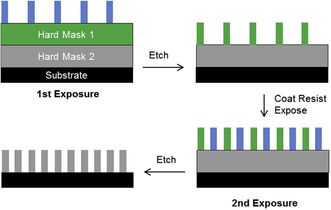
Althoughtherearemanydifferentpotentialwaystoimplementdoubleandmultiplepatterning,34 onlyafewwillbebrieflyreviewedhere.Onemethodisknownas Litho-Etch-Litho-Etch(LELE)anditinvolvestwolithographicexposureandetch stepstocreateasinglelayer.Themethodinvolvesfirstdepositingafilmstackconsistingofoneormorehardmasksontothewafer.Oneexposureisdoneneartheresolutionlimitofthetoolandthispatternisetchedintotheunderlyingfilmstack.A secondexposurepatternthatisoffsetfromthefirstpatternisthencarriedoutand transferredintotheUL.Thecombinedpatternfromthetwodifferentexposuresis atdoublethepitchofeachindividualpattern.Theprocessisdemonstratedin Fig.3.Thisprocesshasanadvantageinthatitcan,intheory,beappliedtoanygeneralpattern,butitishighlysensitivetooverlayerror,whichistheerrorbetweenthe alignmentofeachmasktotheunderlyingpattern.
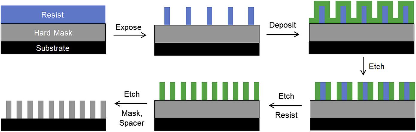
Anothercommonlyusedmethodofdoublepatterningiscalledself-aligneddoublepatterning.35 Itinvolvesthedepositionofaconformalcoatingofafilmontoa singleresistpattern.Thefilmcanthenberemovedbyaselectiveetcheverywhere butonthesidewallsoftheoriginalresist.Theresististhenremovedandtheremainingsidewallpatternwillbeatasmallerpitchandresolutionthantheoriginalresist. Transferofthisremainingsidewallpatternintothesubstratecompletestheprocess. Thismethodisillustratedin Fig.4.ThisprocessisslightlysimplerthanLELEand haslessstringentoverlayerrorrequirements,butisgenerallylimitedtoamore restrictivesetofpatternssuchasalternatinglines.Thisprocesscanalsoberepeated asecondtimeonthefirstsidewallpatternstoeffectivelyquadrupletheoriginalresist pitchinaprocessknownasself-alignedquadruplepatterning.
Multiplepatterningtechniq uesusingdirectedself-assembly(DSA)oforganic materialssuchasblockcopolymers(BCPs)havereceivedmuchinterest.35 43 BCPsarepolymerscomposedoftwoormorediscreteblocksofhomopolymers thatarecovalentlyjoinedtogether;someexamplesofBCPsinclude polystyrene-block-polymethylmethacry late(PS-b-PMMA)orpolystyrene-blockpolydimethylsiloxane(PS-b-PDMS).BCPsareofinterestbecausetheycanphase separatetolengthscalesthatarecommensuratewithdesiredlithographicpatterns. DSAisthemethodwherebytheself-assemblyisspatiallycuedorcontrolledto producelithographicallyusefulphase-se paratedstructuresthatareatasmaller pitchthanisaccessiblefromasingleexposurestep.
FIGURE3
DiagramofLitho-Etch-Litho-Etchprocess.
FIGURE4
Diagramofself-aligneddoublepatterning(SADP)process.
SeveraldifferentwaystocontrolDSAofBCPshavebeeninvestigated44 suchas graphoepitaxy,45 chemoepitaxy,46,47 orvariouscombinationmethods.Achemoepitaxyprocessisillustratedin Fig.5.Conventionallithographyisusedtopatternan ULtoproduceareaswithdifferentchemicalaffinityforeachblockoftheBCP. ThedifferentareascanbeproducedbychemicalmodificationoftheULthrough plasmatreatmentorbyselectiveremovalofareasinthefirstULandadeposition ofanothermaterialsuchasabrushpolymer.Finally,theBCPiscoatedontothe patternedULandannealed.Becauseeachblockhasdifferentaffinityforeach areaoftheUL,specificblocksarealignedtocreatethedirectedself-assembled pattern.MuchprogresshasbeenmadeonevaluatingDSAasapotentialmethod forpitchmultiplication48 andimprovingdefectivity,37,49 however,ithasnotyet beenimplementedindustriallyforcommercialsemiconductorproduction.
Chemoepitaxyprocessflowfordirectedself-assembly(DSA)ofblockcopolymers(BCPs).
1.3.3 EXTREMEULTRAVIOLETLITHOGRAPHY EUVlithographyhasreceivedsubstantialattentioninthelast10þ yearsasa“next wavelength”replacementfor193-nmDUVlithography.11 Overthistime,ithasbeen predictedtobeonlya“few”yearsfromcommercialimplementationmultipletimes, buthasnotyetbeenusedinhighvolumemanufacturing.Partofthisdelayisdueto concernsovertheproductionreadinessofvariousaspectsofthetoolandprocess whichwillbediscussedlater,butalsoduetocontinuedadvancesinmultiple patterningwhichhavekeptpacewiththetechnologyroadmapsuntilnow,although ataveryhigh,andincreasing,cost.
EUVradiationcoversthewavelengthrangefrom10nmuptoabout120nmand alsocanoverlapwitharegionconsideredsoftX-rays.Thewavelengthsthatarethe mostlithographicallyinterestingareintherangeof11 14nm.Consideringthe Raleighcriterionshownin Eq.(1),thiswavelengthrangewouldpotentiallyrepresentasubstantialimprovementinresolutionover193-nmDUV;however,there aremanyimportantdifferencesinthephysicsandtooldesignwhenthewavelength isdroppedintotheEUV.Sinceallmaterialsabsorbatthesewavelengths,thesystem mustberuninavacuumratherthaninairandtransparentopticscannotbeusedin thewayquartzcanbeusedintheDUV.Fortunately,theuseofmultilayerfilmstacks ofalternatingmaterialscanproducereflectingopticswithreasonableefficiency.50 ThemostcommonlyusedEUVreflectorstackconsistsofmultiplealternatinglayers ofmolybdenumandsilicon,whichshowsaround70%reflectionefficiencywitha peakwavelengthof13.5nm.51
EUVexposuretoolsformanufacturingwillrequiremultiplemirrors(6to12þ)to projectasufficientlyhighfidelityimage.Giventhereflectivityof70%foreach mirror,only1 5%ofthegeneratedphotonswillactuallyreachthewafer.This lossmeansthatEUVlightsourcesneedsufficientlyhighpowertoprovidethe requiredwaferthroughputtomakeEUVeconomicallyviable.ProgressinEUV sourcepowerhasbeenslowandhasbeenamongthetop,ifnotthetopconcern/roadblockforimplementationofEUVcommercially.Currentestimatessuggestasource powerof250Wwillbeneededwithlong-termreliableoperation.Asofspring2016, alabdemonstratedpowerof200Whadbeenreported,butsourcesinactualfield demonstrationunitswerearound80W.52 Thelowsourcepoweralsomeansthat EUVresistsneedverygoodsensitivitywhichwillbediscussedlater.
EUVmaskshavealsorequiredsignificantwork.Inadditiontoreflectiveoptics, EUVusesamaskcomposedofareflectivemultilayer.Thereflectivemaskrequires off-axisilluminationandthiscombineswiththeeffectofthethicknessofthemask
FIGURE5
absorbertocreateshadowingeffects,53 whichdegradepatternqualityandmustbe accountedforinmaskandsystemdesign.TheEUVlightthatisreflectedfroma multilayerissomecumulativedistributionofthereflectionsatinterfacesbetween allthelayers.Thisisimportantbecauseitimpliesthatanydefectsburiedinthe multilayercanhaveaneffectontheprojectedpattern.54,55 Thesedefectswillbe difficulttofindusingconventionaldefectanalysisbecausetheywillbeverysmall scaleandpotentiallyinvisibletomanyinspectionmethodsastheyareburied.As aresult,aspecializedtechniquehadtobedevelopedeventoinspectEUVmasks fordefectsbasedonactinicinspection.56 58
AlthoughEUVcanbeconsideredaformofopticallithography,theinteractions ofanEUVphotonwitharesistaresignificantlydifferentthanaDUVphoton,dueto themuchhigherenergyatEUVandthetypicallyhigherabsorbanceatEUV.Anincident13.5-nmEUVphotonhasabout92eVofenergycomparedto5.0and6.4eVfor theDUVwavelengthsof248and193nm,respectively.Thisenergydifference meansthereisasignificantlydifferentphotonfluxontotheresistatequivalentdoses. Thereareapproximately10photons/nm2 atEUVforadoseof15mJ/cm2,while thereare146photons/nm2 attheequivalentdoseat193nm.AtDUV,thephoton isabsorbedbytheresistandittemporarilyexcitesanelectroninamoleculetoan excitedstatebeforereturningtothegroundstate.Whenthe92-eVEUVphotonis absorbedbytheresist,aphotoelectronofabout80eV(onaverage)isgenerated.59 Thephotoelectronwillscatterthroughtheresistandgeneratemoresecondaryelectrons(aroundtwotofivetotalsecondaryelectronsfortypicalorganicresists)ina mannersimilartothecascadeofsecondaryelectronsgeneratedbyscanningelectron microscope(SEM)ore-beamlithographyinteractions.Thechemistryandphysics thatoccurinaresistduringEUVexposurearethereforeasmuchrelatedto e-beamexposureastheyarerelatedtoDUVexposure,althoughitisultimatelya combinationofthetwo.
1.3.4 E-BEAMLITHOGRAPHY E-beamlithographyusesafocusedbeamofelectronstodirectlyexposearesist.The electrongunisoftenatungstenthermionicemissioncathode.23 Thebeamisfocused ontoaverysmallspotsizethatcanbelessthan10nmusingaseriesofcondenser lensesandbeamdeflectioncoils.ComparedtoUV,DUV,andEUVlithography, e-beamlithographyisamasklessformoflithographyinthatitrequiresnomask becausethedeflectorsandcoilsallowarbitrarydeflectionofthefinelyfocused beam.Indeed,e-beamlithographyisthetechniquethatismostcommonlyusedto patternthemasksusedinotherformsoflithography.Theflexibilityofe-beamallowsalmostanyarbitrarygeometrytobeprogrammedandpatterned,although certainapplicationsthatrequirehighfidelityandalignmentincircularpatterns suchasbit-patternedmediawillusemorespecializedtoolsthatallowforacircular rotatingstage.60,61
Amongthemanydifferenttypesofcommonlyusedlithography,e-beamis widelyconsideredtohavethehighestresolution,especiallywhenusing50to 1.3
100þ keVprimaryelectrons.Featuresassmallas5nmandbelowhavebeenfabricatedusinge-beamlithography.62 Althoughe-beamlithographyhasresolutioncapabilitythatfarexceedscurrentproductionDUVtools,ithassignificantlyslower throughput,whichlimitsitsuseinhighvolumecommercialmanufacturing. Throughputforamodernopticallithographyscannerexceedswelloverahundred wafersperhour.Astandardsinglebeame-beamtoolcantakeseveralhoursto exposeasinglewaferanduptoseveraldaysforsomecomplexmasksortemplates. Thistimewillbelongerasthedesiredspotsizeisdecreasedtoimproveresolution. Patterningine-beamcanalsotakemoretimebecausethehighestresolutionresists areoftennonchemicallyamplifiedresistswhichrequiremuchhigherdosesthanthe chemicallyamplifiedresists(CARs)commonlyusedinopticallithography.Thelow throughputhashistoricallylimitede-beamlithographytomaskmakingandresearch anddevelopmentpurposes;however,workhasbeencarriedoutandcontinueson methodsandtooldesignswhichcouldimprovethroughputsuchasprojection e-beam,63 66 multiple-beam,67,68 shape-variablebeam,69 andreflectivebeam.70
Multiple-beame-beamlithographyispotentiallythemostadvancedoptionatthis time,andimprovesthroughputbymassivelyparallelizingthebeamsthatpattern thewafer.71
Themostimportantradiation materialinteractioninopticallithographyatUV andDUVwavelengthsisdirectphotonabsorptiontotemporarilyexciteamolecule toanexcitedstateasdiscussedearlier.Ine-beamlithography,theradiation materialinteractionisverydifferentandisinmanywayssignificantlymorecomplex.72 Highenergyprimaryelectrons(typically50 100keV)enterthetopsurfaceand scatterthroughtheresistbyaseriesofelasticandinelasticcollisions.Theinelastic collisionscausealossofenergyandgeneratemultiplesecondaryelectrons.Thesecondaryelectronscanlikewisescatterthroughtheresistwithsimilarphysicsand generateevenmoreadditionalfreeelectrons.Inthismanner,asingleincidentelectroncangeneratealargecloudofelectrons.Thiscloudofelectronsoftenhasa teardrop-shapedinteractionvolumewiththeresistasshownin Fig.6.Theelectron trajectoriesandsecondaryelectrongenerationcanbesimulatedusingMonteCarlo techniques.73,74
Theelectronswhichscatterthroughtheresistasdescribedearlierandshownin Fig.6 canbeconsideredforwardscatteringoftheelectronsbecausemostoftheelectronsarescatteredatsmallanglesforwardintotheresist.Thereisanotherscattering phenomenonthatisimportantine-beamlithographycalledbackwardscattering. Thisoccurswhenelectronsarescatteredatmuchhigheranglesfromthesubstrate backwardintotheresist.Backwardscatteringismorelikelywhenelectrons encounterhigher Z elementsasarecommonlyfoundintheinorganicsubstrates.It isaconcernbecauseitseffectsarefeltoveramuchlargerdimensionalrange,up tomicronsawayfromtheincidentbeamratherthanthenanometerlengthscale forforwardscattering.Backwardscatteringtendstocausedensefeaturestoreceive ahighereffectivedosethansparsefeaturesbecausethebackwardscatteredelectrons fromneighboringfeaturescontributetothetotaldosewhilethesparsefeatureshave fewneighbors.Thisisknownastheproximityeffect75 andproximityeffect